Application notes


Technical notes
Ask an engineer


Publications
United States (EN)
Select your region or country.
InGaAs linear sensor reference circuit design - Section 6
John Gilmore, Lu Cheng, Hamamatsu Corporation
Scott Hunt, Analog Devices, Inc.
December 15, 2018
Section 1: Introduction
Section 2: System description
Section 3: Analog devices sensor board
Section 4: FPGA/USB processor data path
Section 5: FPGA/USB processor control/status path
Section 6: FPGA design description
Section 7: USB sub-system
Section 8: PC software and IGAA driver library
Section 9: Test results
This technical note is divided into nine sections. To navigate to any section, use the hyperlinks above.
Section 6: FPGA Design Description
The FPGA design is based on Intel (Altera) Cyclone III device EP3C25F324C8. The FPGA design is written in VHDL. The design consists of the major blocks listed in Table 6-1.
Table 6-1 List of the FPGA Modules
| # | Module Name | Source File Name | Description |
|---|---|---|---|
| 1 | top | top.vhd | Top level of the design hierarchy |
| 2 | clock_reset_gen | clock_reset_gen.vhd | Clock and reset generator |
| 3 | control | control.vhd | I2C slave control interface |
| 4 | regs | regs.vhd | Control register bank |
| 5 | detector_con | detector_con.vhd | Sensor controller |
| 6 | adc_con | adc_con.vhd | Controller responsible for U1 (ADAQ7980BCCZ) control and for U4 (AD5235BRUZ25) digital potentiometer control via SPI bus on the ADI circuit card |
| 7 | slavefifo2b_streamin | slavefifof2b_streamin.vhd | Slave FIFO interface to EZ-USB device |
| 8 | ad5627_con | ad_5627_con.vhd | Controller responsible for temperature set-point DAC U9 (AD5627RBRMZ-1) on the ADI circuit card |
| 9 | ad7991_con | ad_7991_con.vhd | Controller responsible for temperature monitoring ADC U10 (AD7991YRJZ-1500) on the ADI circuit card |
| 10 | mpac | mpac.vhd | Multi-Port Access Controller (MPAC) provides shared access of ad_5627_con and ad7991_con to the common I2C bus through I2C_master module |
| 11 | I2C_master | I2C_master.vhd | Provides I2C bus master functionality needed to access I2C slave peripherals on the ADI circuit card |
| 12 | adc_xf | adc_xf.vhd | Provides low-level control of the U1 (ADAQ7980BCCZ) ADC |
| 13 | ddr | ddr.vhd | Altera Megafunction IP providing DDR I/O functionality |
| 14 | I2C_xf | I2C_xf.vhd | I2C Slave interface, used as a part of control module |
| 15 | cbus_con | cbus_con.vhd | As a part of control module, this serves as read and write access bridge between the I2C slave interface and the register bank module (regs) |
| 16 | tx_fifo | tx_fifo.vhd | This is a FIFO that receives its data from adc_con and makes it available to the slavefifof2b_streamin module for transfer to the USB processor. |
| 17 | pll | pll.vhd | Altera Megafunction IP providing PLL functionality used within clock_reset_gen module |
| 18 | N/A | custom.vhd | This serves as the design library. It contains package "custom" which captures commonly used functions, constants and data types. |
The structure of the FPGA design is shown in Figure 6-1.
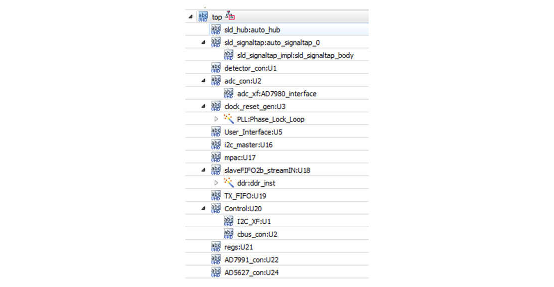
Figure 6-1: FPGA design structure
6A. clock_reset_gen.vhd
Module Inputs and Outputs
Table 6-2 Module I/Os
| Port Name | Type | Direction | Description |
|---|---|---|---|
| clk_in | std_logic | in | 50 MHz clock input |
| reset_n | std_logic | in | Active-low, asynchronous reset input |
| Clock_Divider | std_logic_vector (8 down to 0) | in | Controls the rate at which clk_en_1x and clk_en_2x are generated |
| rst_n | std_logic | out | Active-low, reset output, synchronously de-asserted, asynchronously asserted |
| clk | std_logic | out | 60 MHz clock |
| clk_del | std_logic | out | 60 MHz clock, synchronous to clk, 0 delayed |
| clk2x | std_logic | out | 120 MHz clock, synchronous and aligned to clk |
| clk_en_1ms | std_logic | out | Active-high, single clk cycle wide pulse, every 1 msec |
| clk_en_10ms | std_logic | out | Active-high, single clk cycle wide pulse, every 10 msec |
| clk_en_100ms | std_logic | out | Active-high, single clk cycle wide pulse, every 100 msec |
| clk_en_1x | std_logic | out | Active-high, single clk cycle wide pulse, occurring at a rate of 60 MHz/(2×Clock_Divider) |
| clk_en_2x | std_logic | out | Active-high, single clk cycle wide pulse, occurring at a rate of 60 MHz/(1×Clock_Divider) |
Module IP
Altera ALTPLL Megafunction: PLL, shown in Figure 6-2, generates 60MHz, 120MHz, and 60MHz clocks based on 50MHz clock input.
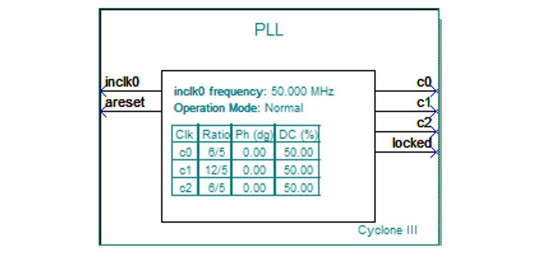
Figure 6-2: Altera ALTPLL megafunction IP providing PLL functionality
Module Description
This module receives 50MHz clock from the Altera Cyclone-III Starter Board (DK-START-3C25N). The received clock is provided to the PLL based on ALTPLL Megafunction IP provided by Altera. The resultant clocks clk, clk_2x and clk_del are generated.
The module receives an asynchronous reset signal "reset_n" and creates asynchronously asserted, synchronously to "clk" de-asserted, active-low reset output "rst_n".
The module generates various clock enable outputs (programmable ones based on Clock_Divider: clk_en_1x and clk_en_2x; fixed ones: at 1msec, at 10msec, at 100msec intervals).
6B. control.vhd
Module Inputs and Outputs
Table 6-3 Module I/Os
| Port Name | Type | Direction | Description |
|---|---|---|---|
| clk_sys | std_logic | in | 60 MHz clock input |
| rst_n | std_logic | in | Active-low, asynchronously reset, synchronously set reset input |
| CBUS_CON_Di | std_logic_vector (7 down to 0) | in | Read Data bus |
| SCL | std_logic | in | I2C clock |
| SDA | std_logic | in, out | I2C data |
| CBUS_CON_A | std_logic_vector (7 down to 0) | out | Register address |
| CBUS_CON_Do | std_logic_vector (7 down to 0) | out | Register write data |
| CBUS_CON_WRS | std_logic | out | Register write strobe, active-high |
| CBUS_Read | std_logic | out | Register read strobe, active-high |
Module Description
The module combines an I2C slave module (I2C_xf) with cbus_con module allowing to perform a write or a read access to a bank of registers connected external to control module. Refer to Figures 6-3 and 6-4.
During I2C write transfers the I2C_xf receives one byte at a time. A typical transfer consists of 2 payload bytes: register address byte, followed by register data byte.
Each received data payload byte is presented at recv_data(7:0) output of the I2C_xf module, while being accompanied by ser_load_en active-high single clock cycle pulse. This indicates to the CBUS controller (cbus_con) that the data is to be stored.
first_byte output from I2C_xf indicates whether the data byte presented to cbus_con represents register address or register data. If first_byte is asserted (active-high single clock cycle pulse) concurrently with data_vld output of I2C_xf, then the data byte is register address, else the data byte is register data to be stored at the respective address location.
During I2C read transfers the I2C_xf module transfers the data presented at xmit_dat(7:0) input onto the I2C bus.
A typical register write transfer is shown in Figure 6-3.

Figure 6-3: Typical I2C write transfer. STA = Start, SA = Slave ACK, STP = Stop, W = Write, X = any value (1 or 0)
The first data byte serves as register address, while the second data byte serves as register write data. A typical register read transfer is shown in Figure 6-4.
Figure 6-4: Typical I2C read transfer. MN = Master NACK, R = Read
A read transaction consists of two separate transfers:
1) The first is a write transfer with first data byte having all zeros, and the second data byte used to indicate the register address to be accessed for a subsequent read transfer.
2) The second is a read transfer with data byte returned by the slave_xf containing the data corresponding to the register address presented during the first step.
Figure 6-5: Control module architecture
6C. I2C_xf.vhd
Module Inputs and Outputs
Table 6-4 Module I/Os
| Port Name | Type | Direction | Description |
|---|---|---|---|
| clk_sys | std_logic | in | 60 MHz clock input |
| rst_n | std_logic | in | Active-low, asynchronously reset, synchronously set reset input |
| SDA_in | std_logic | in | I2C SDA input |
| SDA_out | std_logic | in | I2C SDA output |
| SDA_oeN | std_logic | in | I2C SDA output enable, active-low |
| SCL | std_logic | in | I2C SCL input |
| I2C_A | std_logic_vector (7 down to 1) | in | I2C Slave address |
| data_vld | std_logic | out | Active-high, single clk_sys wide pulse, indicating that recv_data(7:0) is valid |
| recv_dat | std_logic_vector (7 down to 0) | out | Data payload byte received via I2C |
| load_en | std_logic | out | Indicates that the data byte has been loaded into transmit register (used for read transfers) |
| xmit_dat | std_logic_vector (7 down to 0) | in | Data to be transmitted on I2C bus |
| first_byte | std_logic | out | Indicates the first data payload byte within an I2C write stream |
| cbus_dir | std_logic | out | CBUS direction transfer: 0 = Write, 1 = Read |
| addr_incr | std_logic | out | Used during read transfers, this active-high signal produces a single clk_sys cycle wide pulse each time a payload byte has been transferred via I2C interface. |

Figure 6-6: I2C module I/Os
Module Description
This module implements the physical access to the I2C bus. The module acts as an I2C slave with slave address passed via I2C_A port. The module responds to 8-bit slave address of 0xAA/0xAB. The I2C interface supports I2C clock rates of up to 400KHz.
The I2C module design is based on a finite state machine (FSM). The FSM is shown in Figure 6-7.
The FSM dwells in IDLE state until start is detected on the I2C bus. The FSM proceeds through A7_ST to A0_ST states receiving one address bit at a time with each falling edge of SCL. Upon arriving to ADDR state the received address is compared to the device address (0xAA/0xAB). If the upped 7 bits match, the slave asserts acknowledge and proceeds to receive a data byte (states D7_ST through D0_ST). Each bit of the data byte is received on the falling edge of the SCL line.
SCL_fedge represents a falling edge of I2C SCL clock received by the FPGA. All other conditional signals are self-explanatory.
Figure 6-7: I2C state machine
6D. cbus_con.vhd
Module Inputs and Outputs
Table 6-5 Module I/Os
| Port Name | Type | Direction | Description |
|---|---|---|---|
| clk_sys | std_logic | in | 60 MHz clock input |
| rst_n | std_logic | in | Active-low, asynchronously reset, synchronously set reset input |
| ser_data_vld | std_logic | in | Single clock wide, active-high, signal indicating that a serial byte has been received and it is ready to be stored |
| ser_addr_incr | std_logic | in | For multi-byte transfers (write or read), this single clock cycle wide, active-high signal indicates that the next register address access should be started |
| ser_first_byte | std_logic | in | Single clock wide, active-high, signal indicating that the byte being received is the first byte, which represents CRDR address, while the second byte is the read register address. This signal is used for read transfers only. |
| ser_cbus_wr | std_logic | in | Single clock wide, active-high, signal indicating a CBUS write transaction |
| ser_recv_data | std_logic_vector (7 down to 1) | in | A data byte received from the I2C interface |
| ser_load_en | std_logic | in | Active-high, single clk_sys wide pulse, indicating used in conjunction with ser_addr_inc signal to cause an address on the CBUS to be incremented |
| ser_xmit_data | std_logic_vector (7 down to 0) | out | Data to be transmitted on the I2C bus |
| CBUS_Read | std_logic | out | Active-high, single clk_sys wide pulse, used a read enable on the CBUS |
| CBUS_WRS | std_logic | out | Active-high, single clk_sys wide pulse, used a write enable on the CBUS |
| CBUS_A | std_logic_vector (7 down to 0) | out | CBUS address |
| CBUS_Do | std_logic_vector (7 down to 0) | out | CBUS write data |
| CBUS_Di | std_logic_vector (7 down to 0) | in | CBUS read data |
Figure 6-8: CBUS_CON module I/Os
Module Description
cbus_con module receives raw bytes from the I2C_xf module and interprets them into register read and write accesses. Once interpreted, the module produces address (CBUS_A), write data (CBUS_Do) and write strobe (CBUS_WRS) signals to the downstream register bank for a write transaction; or (CBUS_A) and read strobe (CBUS_Read) for a read transaction. The read data is CBUS_Di.
The module also transfers the read data back to I2C_xf module for a transfer back to I2C master via the serial bus.
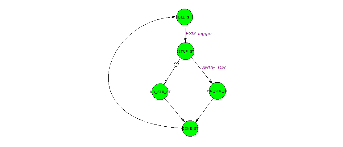
Figure 6-9: CBUS_CON state machine
6E. regs.vhd
Module Inputs and Outputs
Table 6-6 Module I/Os
| Port Name | Type | Direction | Description |
|---|---|---|---|
| clk_sys | std_logic | in | 60 MHz clock input |
| rst_n | std_logic | in | Active-low, asynchronously reset, synchronously set reset input |
| CBUS_Read | std_logic | in | Active-high, single clk_sys wide pulse, used a read enable on the CBUS |
| CBUS_WRS | std_logic | in | Active-high, single clk_sys wide pulse, used a write enable on the CBUS |
| CBUS_A | std_logic_vector (7 down to 0) | in | CBUS address |
| CBUS_Do | std_logic_vector (7 down to 0) | in | CBUS write data |
| CBUS_Di | std_logic_vector (7 down to 0) | out | CBUS read data |
| iREG_0C through iREG_19 |
std_logic_vector (7 down to 0) | in | These represent inputs for the readable registers at addresses 0x0C through 0x19 |
| REG_00 through REG_2F |
std_logic_vector (7 down to 0) | out | These mirror the contents of the writable registers at addresses 0x00 through 0x2F |
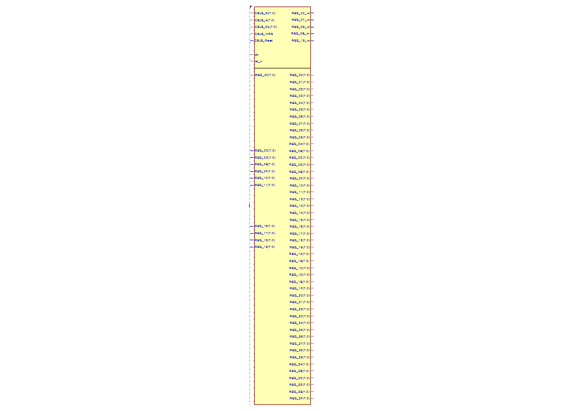
Figure 6-10: regs module I/Os
Module Description
regs module provides access to the contents of the registers at addresses 0x00 through 0x2F.
When a read transfer in the range from 0x0C to 0x19 is requested, the contents of iREG_0C through iREG_19 is used.
Read access to the address range 0x0C to 0x11 is mapped to AD7991 ADC channel 0 through 2.
REG_00 to REG_2F provide control over the various functions of the FPGA.
6F. detector_con.vhd
Module Inputs and Outputs
Table 6-7 Module I/Os
| Port Name | Type | Direction | Description |
|---|---|---|---|
| clk_sys | std_logic | in | 60 MHz clock input |
| rst_n | std_logic | in | Active-low, asynchronously reset, synchronously set reset input |
| clk_en_2x | std_logic | in | Active-high, clock enable at a rate equal to 60 MHz/Clock_Divider (refer to Table 6-2) The default value of Clock_Divider is 10, resulting in 6 MHz rate of clk_en_2x |
| clk_en_1x | std_logic | in | Active-high, clock enable at a rate equal to 60 MHz/(2 x Clock_Divider) (refer to Table 6-2) The default value of Clock_Divider is 10, resulting in 3 MHz rate of clk_en_1x |
| op_en | std_logic | in | Active-high signal, when set enable the operation of the sensor controller |
| Integration_Time | std_logic_vector (31 down to 0) | in | This input controls the integration time in units of 60 MHz/(2 x Clock_Divider). The default value is 0x00000339, resulting in 275 µsec default integration time. |
| reset_odd | std_logic | out | Odd reset output to the image sensor |
| clk_odd | std_logic | out | Odd clock output to the image sensor |
| adtrig_odd | std_logic | in | ADC odd pixel trigger input from the image sensor |
| reset_even | std_logic | out | Even reset output to the image sensor |
| clk_even | std_logic | out | Even clock output to the image sensor |
| adtrig_even | std_logic | in | ADC even pixel trigger input from the image sensor |
| adtrig_odd_test | std_logic | out | Test output. Emulates the corresponding trigger input. |
| adtrig_even_test | std_logic | out | Test output. Emulates the corresponding trigger input. |
| pix_mode | std_logic | in | Pixel mode: 0 = 256 pixel mode (default) 1 = 512 pixel mode |
| hs_mode | std_logic | in | Sensor interface speed: 0 = Regular speed mode (default) 1 = High speed mode |
| par_mode | std_logic | in | Parallel mode: 0 = Sequential op mode (default) 1 = Parallel op mode (odd and even pixels are clocked concurrently and slower) |
| mux_con_inv | std_logic | in | Pixel multiplexor control: 1 = Invert even_odd_n 0 = Do not invert (default) |
| even_odd_n | std_logic | out | Multiplexor control: 0 = Odd data select 1 = Even data select |
| sync | std_logic_vector (1 down to 0) | out | This signal is used to indicate to Slave FIFO interface the beginning of the integration phase of sensor control "01": Integration started "10": Integration started 1 cycle ago "00": Integration not started "11": Reserved/Invalid |
| adc_trigger | std_logic | out | Test output for ADC controller (emulates that of the image sensor) |
| last_xfer | std_logic | out | Active-high, single clk wide signal: 1: Marks the moment when the last pixel burst is starting |
| integr_start | std_logic | out | Active-high, single clk wide signal: 1: Marks the beginning of the integration interval |
| integr_end | std_logic | out | Active-high, single clk wide signal: 1: Marks the end of the integration interval |
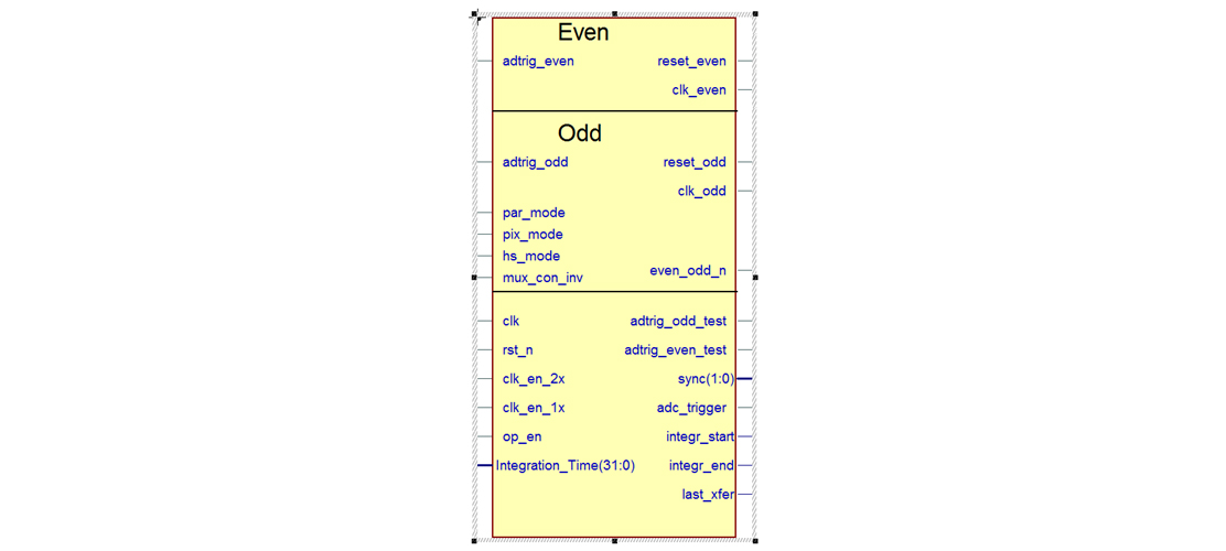
Figure 6-11: detector_con module I/Os
Module Description
The detector controller module provides the logic and timing for the control signals needed to properly control a detector device under test.
The controller supports the following operating modes:
- 256 or 512 pixels
- Regular or High-speed operation
- Normal (Sequential) or Parallel operating mode
Figure 6-12 through Figure 6-28 demonstrate the relationship between the detector control signals in all possible operating modes.
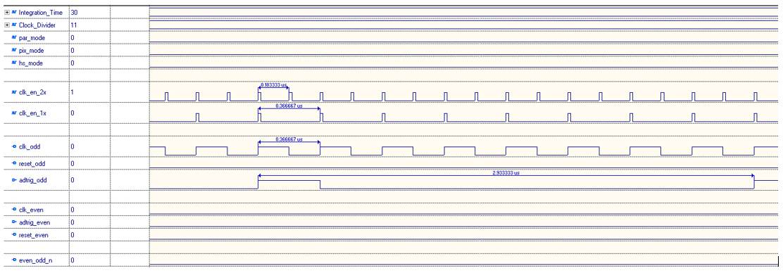
Figure 6-12: 256-pixel, regular speed, sequential mode timing
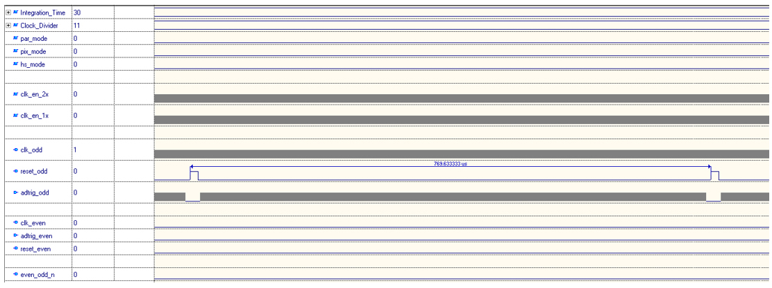
Figure 6-13: 256-pixel, regular speed, sequential mode operation
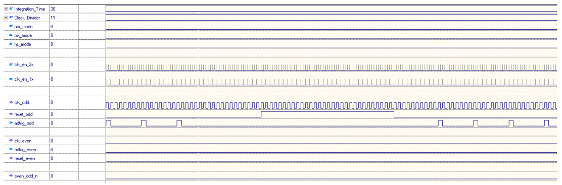
Figure 6-14: 256-pixel, regular speed, sequential mode operation around reset
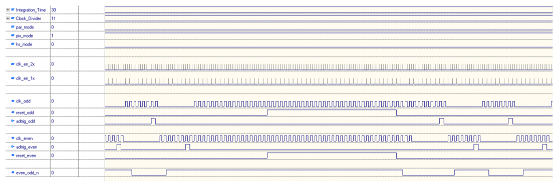
Figure 6-15: 512-pixel, regular speed, sequential mode operation around reset
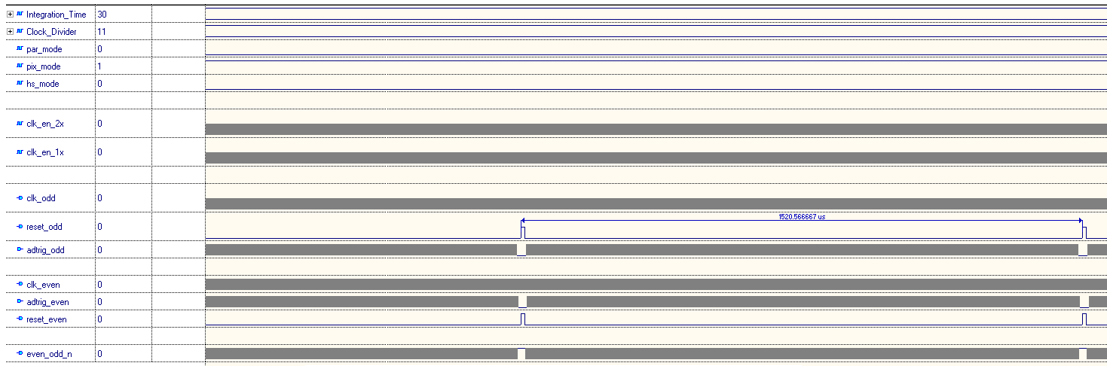
Figure 6-16: 512-pixel, regular speed, sequential mode operation overview
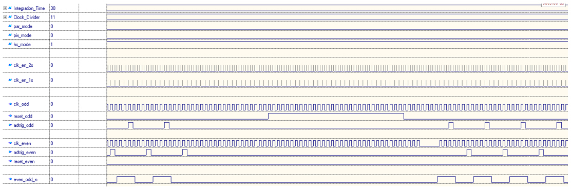
Figure 6-17: 256-pixel, high speed, sequential mode operation around reset
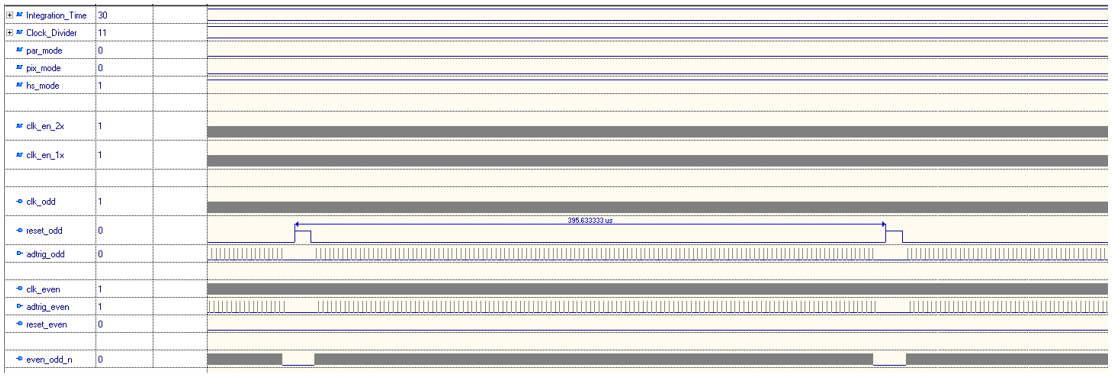
Figure 6-18: 256-pixel, high speed, sequential mode operation overview
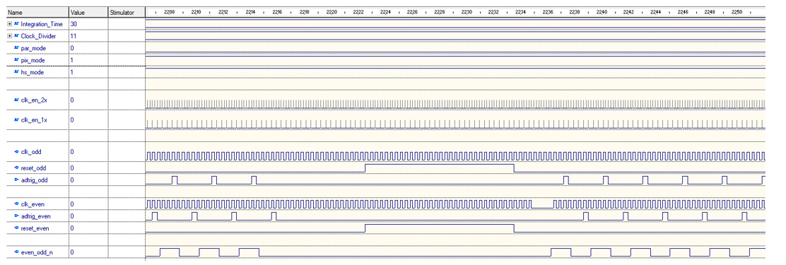
Figure 6-19: 512-pixel, high speed, sequential mode operation around reset
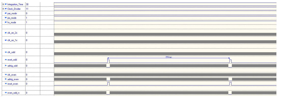
Figure 6-20: 512-pixel, high speed, sequential mode operation overview
Figure 6-21: 256-pixel, regular speed, parallel mode operation around reset
Figure 6-22: 256-pixel, regular speed, parallel mode operation overview
Figure 6-23: 512-pixel, regular speed, parallel mode operation around reset
Figure 6-24: 512-pixel, regular speed, parallel mode operation overview
Figure 6-25: 256-pixel, high speed, parallel mode operation around reset
Figure 6-26: 256-pixel, high speed, parallel mode operation overview
Figure 6-27: 512-pixel, high speed, parallel mode operation around reset
Figure 6-28: 512-pixel, high speed, parallel mode operation overview
The detector controller module design is based on an FSM (Finite State Machine) shown in Figure 6-29.
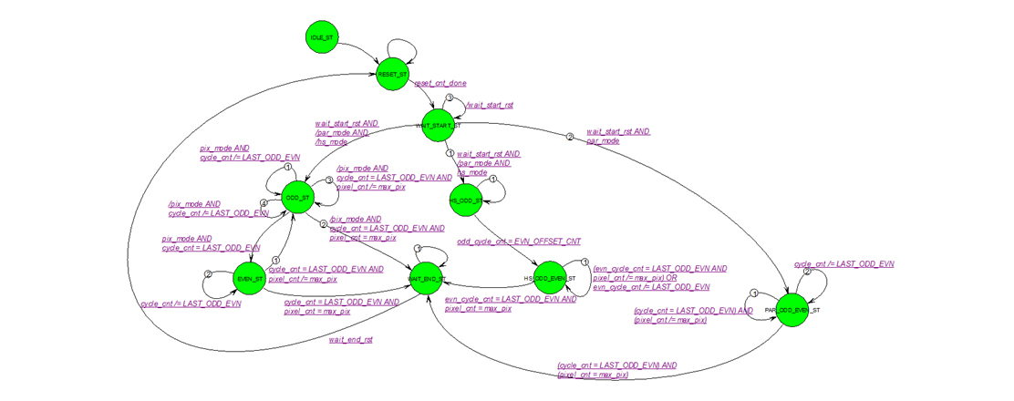
Figure 6-29: Detector controller state machine
6G. adc_con.vhd
Module Inputs and Outputs
Table 6-8 Module I/Os
| Port Name | Type | Direction | Description |
|---|---|---|---|
| clk | std_logic | in | 60 MHz clock input |
| clk_del | std_logic | in | 60 MHz clock input |
| clk_2x | std_logic | in | 60 MHz clock phase shifted by 0 deg from clk |
| rst_n | std_logic | in | Active-low, asynchronously reset, synchronously set reset input |
| clk_en | std_logic | in | 100 msec clock enable, active-high, 1 clk long |
| mosi | std_logic | out | SPI data output (Master Out Slave In) |
| miso | std_logic | in | SPI data input (Master In Slave Out) |
| sclk | std_logic | out | SPI clock output |
| adc_conv | std_logic | out | ADAQ7980 CNV signal, active-high |
| digipot_cs_n | std_logic | out | Digital potentiometer AD5235 Chip Select, active-low |
| digipot_rdy | std_logic | in | Digital potentiometer AD5235 read data ready, active-high, 1 clk wide |
| digipot1_wr | std_logic | in | AD5235 digital potentiometer 1 write command, active-high, 1 clk wide |
| digipot2_wr | std_logic | in | AD5235 digital potentiometer 2 write command, active-high, 1 clk wide |
| RDAC1 | std_logic_vector(9:0) | in | AD5235 digital potentiometer 1 write data |
| RDAC2 | std_logic_vector(9:0) | in | AD5235 digital potentiometer 2 write data |
| RDAC1_rd_data | std_logic_vector(9:0) | out | AD5235 digital potentiometer 1 read data |
| RDAC2_rd_data | std_logic_vector(9:0) | out | AD5235 digital potentiometer 2 read data |
| pg_en | std_logic | in | Pattern Generator Enable, active-high |
| last_xfer | std_logic | in | Last Transfer indicator, active-high |
| integr_end | std_logic | in | Integration End indicator, active-high, 1 clk wide |
| integr_start | std_logic | in | Integration Start indicator, active-high, 1 clk wide |
| adc_data | std_logic_vector(15:0) | out | ADAQ7980 data output |
| data_rdy | std_logic | out | ADAQ7980 data ready, active-high, 1 clk wide |
| adc_trigger | std_logic | in | Trigger for ADAQ7980 ADC conversion, active-high, 1 clk wide |
Figure 6-30: adc_con module I/Os
Module Description
adc_con module serves as an interface between the FPGA and the two Analog Devices ICs sharing the same SPI bus: ADAQ7980 (ADC) and AD5235 (Dual Digital Potentiometer). adc_con module includes adc_xf module, which implements the interface logic, while adc_con serves the functions of a wrapper and contains some glue logic. As the SPI interface is shared, the design of the adc_xf includes an arbiter, allowing access to both physical devices using the shared interface.
6H. adc_xf.vhd
Module Inputs and Outputs
Table 6-9 Module I/Os
| Port Name | Type | Direction | Description |
|---|---|---|---|
| clk | std_logic | in | 60 MHz clock input |
| clk_del | std_logic | in | 60 MHz clock input |
| clk_2x | std_logic | in | 60 MHz clock phase shifted by 0 deg from clk |
| rst_n | std_logic | in | Active-low, asynchronously reset, synchronously set reset input |
| clk_en | std_logic | in | 100 msec clock enable, active-high, 1 clk long |
| mosi | std_logic | out | SPI data output (Master Out Slave In) |
| miso | std_logic | in | SPI data input (Master In Slave Out) |
| sclk | std_logic | out | SPI clock output |
| adc_cnv | std_logic | out | ADAQ7980 CNV signal, active-high |
| digipot_cs_n | std_logic | out | Digital potentiometer AD5235 Chip Select, active-low |
| digipot_rdy | std_logic | in | Digital potentiometer AD5235 read data ready, active-high, 1 clk wide |
| digipot1_wr | std_logic | in | AD5235 digital potentiometer 1 write command, active-high, 1 clk wide |
| digipot2_wr | std_logic | in | AD5235 digital potentiometer 2 write command, active-high, 1 clk wide |
| RDAC1 | std_logic_vector(9:0) | in | AD5235 digital potentiometer 1 write data |
| RDAC2 | std_logic_vector(9:0) | in | AD5235 digital potentiometer 2 write data |
| RDAC1_rd_data | std_logic_vector(9:0) | out | AD5235 digital potentiometer 1 read data |
| RDAC2_rd_data | std_logic_vector(9:0) | out | AD5235 digital potentiometer 2 read data |
| pg_en | std_logic | in | Pattern Generator Enable, active-high |
| last_xfer | std_logic | in | Last Transfer indicator, active-high |
| integr_end | std_logic | in | Integration End indicator, active-high, 1 clk wide |
| integr_start | std_logic | in | Integration Start indicator, active-high, 1 clk wide |
| data | std_logic_vector(15:0) | out | ADAQ7980 data output |
| ready | std_logic | out | ADAQ7980 data ready, active-high, 1 clk wide |
| adc_trigger | std_logic | in | Trigger for ADAQ7980 ADC conversion, active-high, 1 clk wide |
Module Description
adc_xf module serves as an interface between the FPGA and the two Analog Devices ICs sharing the same SPI bus: ADAQ7980 (ADC) and AD5235 (Dual Digital Potentiometer). adc_xf module implements the interface logic based on state machines. As the SPI interface is shared, the design of the adc_xf includes an arbiter, allowing access to both physical devices using the shared interface. The arbitration is based on the fact control coming from the detector_con module.
During the time when odd/even clocks and strobes are actively generated and odd/even trigger inputs are output by the sensor (adtrig_odd/ad_trig_even) the adc_xf communicates with ADAQ7980 to acquire the corresponding pixel data. During the reset intervals, when the sensor is performing integration, adc_xf allows the Read and Write accesses to the digital potentiometer AD5235. The accesses to the digital potentiometer are suspended while the accesses to ADC continue following the integration interval.
The ADC state machine is shown in Figure 6-31. The FSM idles in ADC_IDLE_ST state waiting for the next rising edge of adc trigger from the sensor. adc_tcnv_cnt is initialized to 60; hence the state machine waits in ADC_CNV_ST until the conversion is finished. The wait time is 60 x 60MHz periods, or 1000nsec. ADAQ7980 device conversion time ranges from 500 to 710nsec. With 1000nsec conversion time allowance, the design provides for an ample margin.
Figure 6-31: ADC state machine
The interface to ADC consists of the SPI (with MOSI and Chip-Select not connected) and CNV signal (adc_cnv). During ADC_RD_SNV_RESULT state the 16-bit ADC data is serially captured, while the adc_xf pulses SPI clock SCLK.
The digital potentiometer state machine is shown in Figure 6-32.
Figure 6-32: Digital potentiometer state machine
The digital potentiometer read and write requests are received via I2C and result in the corresponding trigger requests being generated. In response to the trigger requests, while the detector controller is in the reset (integration) phase, the accesses to the digital potentiometer are performed.
6I. AD7991_con.vhd
Module Inputs and Outputs
Table 6-10 Module I/Os
| Port Name | Type | Direction | Description |
|---|---|---|---|
| clk_sys | std_logic | in | 60 MHz clock input |
| rst_n | std_logic | in | Active-low, asynchronously reset, synchronously set reset input |
| clk_en | std_logic | in | 100 msec clk enable, 1 clk wide, active-high |
| xfer_ack_n | std_logic | in | Transfer acknowledge, 1 clk wide, active-low |
| rd_data | array (0 to 15) of std_logic_vector (7 down to 0) | in | Data returned by the AD7991 device |
| error | std_logic | in | Error indicator, returned by the MPAC |
| xfer_req_n | std_logic | out | Transfer request, 1 clk wide, active-low |
| xfer_rw | std_logic | out | Transfer type select, 0 = Write, 1 = Read |
| xfer_size | natural | out | Indicates the number of payload bytes to be transferred |
| xfer_addr | std_logic_vector (7 down to 1) | out | Indicates the I2C slave address to be accessed In the case of AD7991, this is set to "0101001" |
| wr_data | array (0 to 15) of std_logic_vector (7 down to 0) | out | Payload data to be written out to the slave device |
| skip_wr | std_logic | out | Setting this to 1 results in I2C read access performed without write access being done first. |
| ADC_CH0 | std_logic_vector (11 down to 0) | out | Data read from Channel 1 of the ADC |
| ADC_CH1 | std_logic_vector (11 down to 0) | out | Data read from Channel 2 of the ADC |
| ADC_CH2 | std_logic_vector (11 down to 0) | out | Data read from Channel 3 of the ADC |
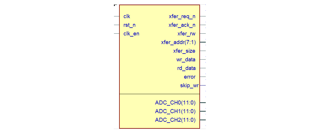
Figure 6-33: AD7991_con module I/Os
Module Description
AD7991_con module is responsible for high-level control of the AD7991 I2C ADC. The system contains 2 I2C devices: AD7991 12-bit ADC and AD5627 12-bit DAC. Both devices share the same I2C bus. To allow for the FPGA to access both devices the design includes a Multi-Port Access Controller (MPAC), connected to I2C Master at one side and to the two I2C controllers (AD7991_con and AD5627_con) on the other side.
AD7991_con controls the high-level I2C commands and data issued to and received from the DAC. The control is based on a state machine shown in Figure 6-34.
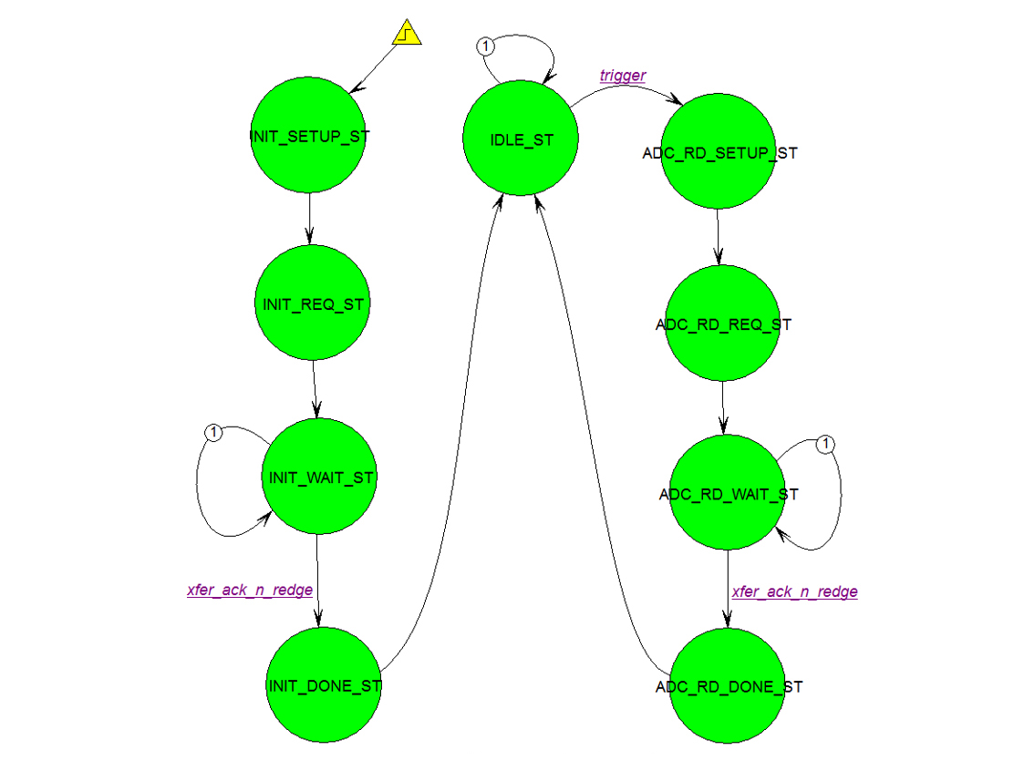
Figure 6-34: AD7991_con state machine
During the initialization phases of the state machine (INIT_SETUP_ST through INIT_DONE_ST), the AD7991 is initialized by performing the following transactions:
Write 00111000 to enable reading Ch0 and Ch1, Select External REF, Enable I2C filtering, Enable bit try and Sample Delay.
Upon completion of the initialization the controller is ready to access the ADC. The ADC read requests are performed via slave I2C interface, when the external USB controller accesses the respective FPGA slave registers. In response, the controller state machine traverses states ADC_RD_SETUP_ST through ADC_RD_DONE_ST and reads the three available analog channels.
6J. AD5627_con.vhd
Table 6-11 Module I/Os
| Port Name | Type | Direction | Description |
|---|---|---|---|
| clk_sys | std_logic | in | 60 MHz clock input |
| rst_n | std_logic | in | Active-low, asynchronously reset, synchronously set reset input |
| clk_en | std_logic | in | 100 msec clk enable, 1 clk wide, active-high |
| DAC | std_logic_vector(11:0) | in | Data to be written to DAC |
| DAC_update | std_logic | in | Trigger, active-high, 1 clk wide resulting in data being sent to the DAC |
| xfer_req_n | std_logic | out | Transfer request, 1 clk wide, active-low |
| xfer_ack_n | std_logic | in | Transfer acknowledge, 1 clk wide, active-low |
| xfer_rw | std_logic | out | Transfer type select, 0 = Write, 1 = Read |
| xfer_addr | std_logic_vector (7 down to 1) | out | Indicates the I2C slave address to be accessed In the case of AD5627, this is set to "0001110" |
| xfer_size | natural | out | Indicates the number of payload bytes to be transferred |
| wr_data | array (0 to 15) of std_logic_vector (7 down to 0) | out | Payload data to be written out to the slave device |
| rd_data | array (0 to 15) of std_logic_vector (7 down to 0) | out | Data read out from the slave device |
| error | std_logic | in | Error indicator, returned by the MPAC |
| skip_wr | std_logic | out | Setting this to 1 results in I2C read access performed without write access being done first. |
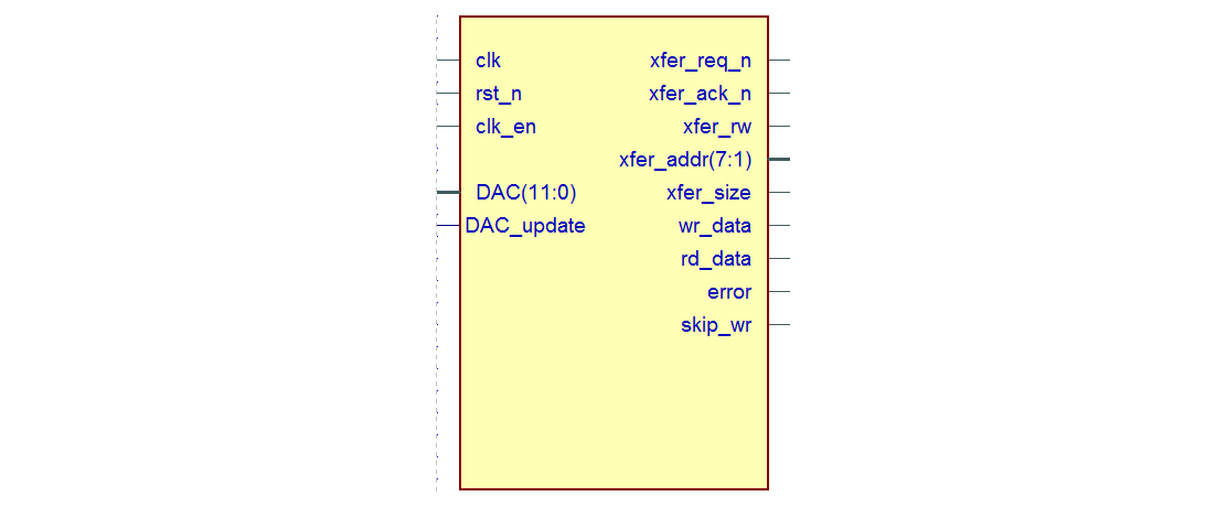
Figure 6-35: AD5627_con module I/Os
Module Description
AD5627_con module is responsible for the initialization and high-level control, including data reads and writes of the AD5627 I2C DAC. All accesses to the physical DAC are performed via I2C bus, using I2C master and a Multi-Port Access Controller (MPAC). The accesses to AD5627 are shared with I2C transfers performed in the course of accesses to AD7991, and therefore are arbitrated by the MPAC. The controller is based on a state machine shown in Figure 6-36.
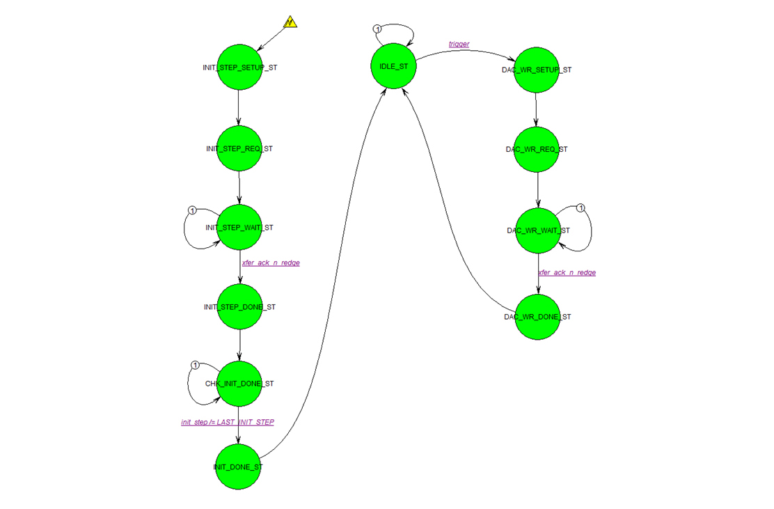
Figure 6-36: AD5627_con state machine
AD5627 initialization consists of 4 steps:
1. LDAC Setup:
a. Data Byte 1 = "00110000" (Command = "110")
b. Data Byte 2 = "00000000" (Don't Care)
c. Data Byte 3 = "00000001" (DAC B LDAC pin enabled, DAC A LDAC pin disabled)
2. Reference Setup:
a. Data Byte 1 = "00111000" (Command = "111")
b. Data Byte 2 = "00000000" (Don't Care)
c. Data Byte 3 = "00000001" (Internal Reference ON)
3. Load Input Shift Register:
a. Data Byte 1 = "01011000" (Byte Selection (S) = 1, Command = "011" (Write to and Update DAC Channel n), DAC Address = "000" (DAC A))
b. Data Byte 2 = DAC(11:4)
c. Data Byte 3 = DAC(3:0) & "0000"
4. Power-up:
a. Data Byte 1 = "00100000" (Command = Power-up)
b. Data Byte 2 = "00000000" (Don't Care)
c. Data Byte 3 = "00000001" (Normal Operation (5:4) = "00", Select DAC A (bit 0 = '1'))
For all subsequent accesses DAC write is performed whenever a trigger is received. Upon a trigger, which is an I2C slave write to the FPGA from the USB sub-system, the state machine sends the 12-bit DAC input to AD5627 device.
6K. mpac.vhd
Module Inputs and Outputs
Table 6-12 Module I/Os
| Port Name | Type | Direction | Description |
|---|---|---|---|
| clk_sys | std_logic | in | 60 MHz clock input |
| rst_n | std_logic | in | Active-low, asynchronously reset, synchronously set reset input |
| xfer_req_n | std_logic_vector(7:0) | in | Active-low transfer request. The request bit is asserted until a corresponding acknowledgement response xfer_ack_n bit is received. |
| xfer_rw | std_logic_vector(7:0) | in | Transfer direction: Read = 1, Write = 0 |
| xfer_addr | array (7:0) of std_logic (7:0) | in | I2C slave address, one for each corresponding port number |
| wr_data | array (7:0) of array (15:0) of std_logic (7:0) | in | I2C payload, 16x8 array for each port |
| xfer_size | array (7:0) of natural | in | Transfer size (number of payload bytes), one value for each respective port |
| skip_wr | std_logic_vector(7:0) | in | If write is not needed before reads take place, this bit indicates that when set. One bit for each of the 8 ports. |
| xfer_ack_n | std_logic_vector(7:0) | in | Transfer acknowledge, active-low, 1 clk wide. Indicates that the requested transfer has been completed. |
| rd_data | array (15:0) of std_logic (7:0) | in | Data read from the I2C slave device |
| error | std_logic_vector(7:0) | in | Error indication, one for each port |
| I2C_xfer_req_n | std_logic | out | Output to the I2C master, active-low, 1 clk wide, requesting a data transfer |
| I2C_addr | std_logic_vector(7:1) | out | Address of the I2C slave device to be accessed |
| I2C_rw | std_logic | out | Transfer direction: 0 = Write, 1 = Read |
| I2C_xfer_size | natural | out | Number of payload bytes to be transferred |
| I2C_wr_data | array (15:0) of std_logic (7:0) | out | Payload bytes to be transferred |
| I2C_rd_data | array (15:0) of std_logic (7:0) | in | Data read as a result of the I2C read transfer |
| I2C_rd_vld | std_logic | in | Active-high, 1 clk wide, indicates that I2C data read is valid |
| I2C_busy | std_logic | in | Indication from the I2C master that a transfer is in progress, active-high |
| I2C_error | std_logic | in | I2C transfer error indication |
| I2C_skip_wr | std_logic | out | If write is not needed before reads take place, this bit indicates that when set. |
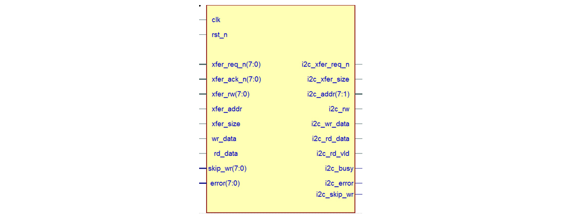
Figure 6-37: MPAC module I/Os
Module Description
The Multi-Port Access Controller links the high-level controllers needing to perform high-level I2C transfers with a single I2C Master controller available on the FPGA. AD7991_con and AD5627_con controllers utilize 2 of the 8 available ports on the MPAC. The MPAC performs round-robin access arbitration between all 8 ports. In reality, since only 2 ports are utilized the available bandwidth is split ~50/50 between the two controllers.
The MPAC design is based on 2 state machines: one state machine is used for round-robin access arbitration, while the second state machine is used for control of the interface with the I2C master module I2C_master.
The arbitration state machine is shown in Figure 6-38. A request is checked one at a time. If a request is asserted, the corresponding port is allowed access to the I2C Master interface via the I2C Master Interface state machine shown in Figure 6-39.
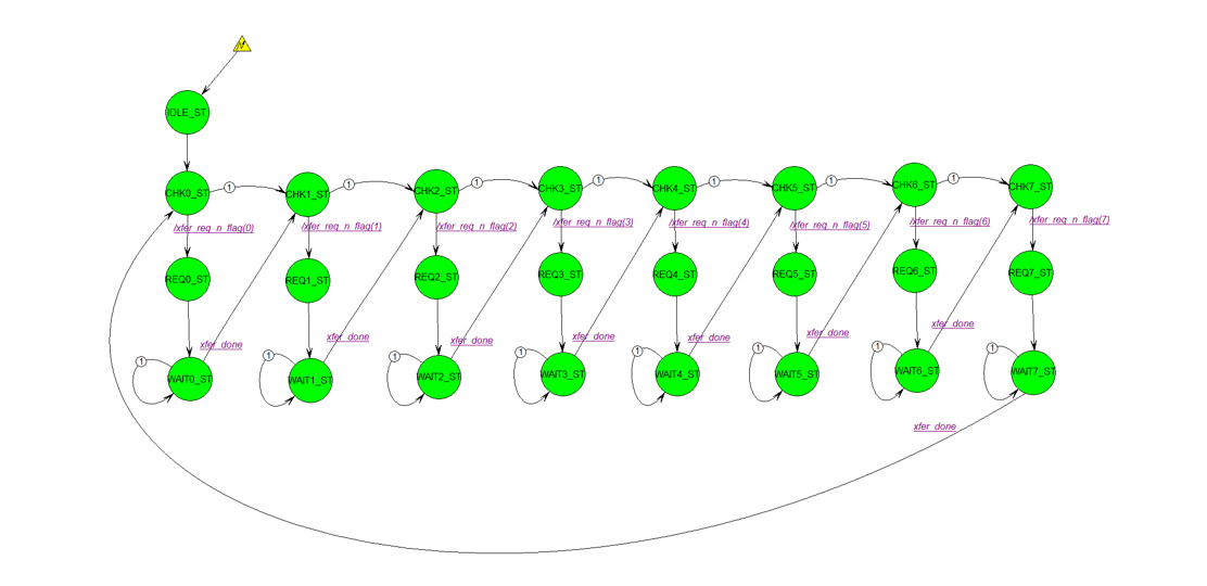
Figure 6-38: MPAC arbitration state machine
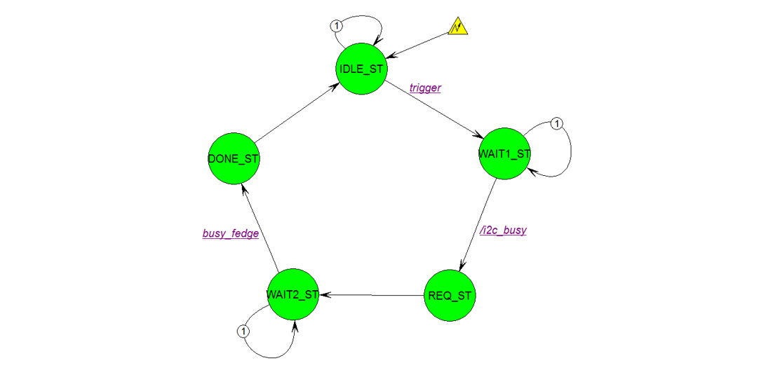
Figure 6-39: MPAC I2C master interface state machine
6L. I2C_master.vhd
Module Inputs and Outputs
Table 6-13 Module I/Os
| Port Name | Type | Direction | Description |
|---|---|---|---|
| clk | std_logic | in | 60 MHz clock input |
| rst_n | std_logic | in | Active-low, asynchronously reset, synchronously set reset input |
| xfer_req_n | std_logic | in | Active-low, 1 clk wide, request to perform a transfer |
| xfer_size | natural range 1 to 16 | in | Payload size in number of bytes |
| addr | std_logic_vector(7:1) | in | Address of the slave device to be accessed |
| rw | std_logic | in | Read/write indication: 0 = Write, 1 = Read |
| data_wr_arr | array (0 to 15) of std_logic_vector(7 down to 0) | in | Array containing the payload data |
| skip_wr | std_logic | in | Set to 1 when a read transfer does not need to be preceded by a write. |
| scl | std_logic | in, out | I2C Clock |
| sda | std_logic | in, out | I2C Data |
| busy | std_logic | out | 1 = I2C Master is busy 0 = I2C Master is ready for the next transfer request |
| ack_error | std_logic | out | 1 = Indicates slave did not acknowledge the transfer |
| data_rd_vld | std_logic | out | 1 = Indicates that the data_rd_arr contains the data |
| data_rd_arr | array (0 to 15) of std_logic_vector (7 down to 0) | out | Data returned during a read transfer |

Figure 6-40: I2C master module I/Os
Module Description
This module interfaces to MPAC module and provides for master access to the I2C bus. The two slave devices accessed by the master are AD7991 and AD5627. The module design is based on a state machine shown in Figure 6-41.
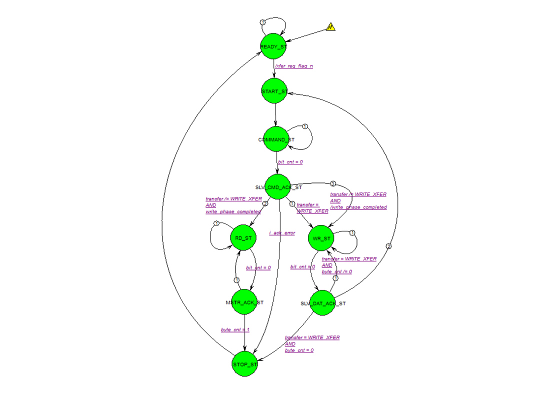
Figure 6-41: I2C master state machine
6M. tx_fifo.vhd
Module Inputs and Outputs
Table 6-14 Module I/Os
| Port Name | Type | Direction | Description |
|---|---|---|---|
| clk | std_logic | in | 60 MHz clock input |
| rst_n | std_logic | in | Active-low, asynchronously reset, synchronously set reset input |
| din | std_logic_vector(15:0) | in | 16-bit pixel data from the A/D converter, FIFO data input |
| wr_en | std_logic | in | FIFO write enable, active-high |
| sync | std_logic_vector(1:0) | in | "01" indicates the beginning of the reset state (integration start) |
| dout | std_logic_vector(15:0) | out | FIFO data output |
| rd_en | std_logic | in | FIFO read enable, active-high |
| rd_vld | std_logic | out | FIFO read data valid, active-high |
| empty | std_logic | out | FIFO empty indication 1 = FIFO is empty |
| full | std_logic | out | FIFO full indication 1 = FIFO is full |
| flag | std_logic | out | FIFO data ready flag 1 = Data is ready for reading from FIFO |
| data_cnt | std_logic | out | FIFO fullness count: indicates the number of 16-bit words available for reading |

Figure 6-42: tx_fifo module I/Os
Module Description
This module serves the purpose of storing the data received from the image sensor prior to having that data transferred to the USB microprocessor via slavefifo2b_streamin module. The FIFO size is 256 words deep, with each word being 16-bits wide.
6N. slavefifo2b_streamin.vhd
Module Inputs and Outputs
Table 6-15 Module I/Os
| Port Name | Type | Direction | Description |
|---|---|---|---|
| clk | std_logic | in | 60 MHz clock input |
| rst_n | std_logic | in | Active-low, asynchronously reset, synchronously set reset input |
| op_en | std_logic | in | Operation Enable Connected to REG01 bit 6 1 = Operation enabled |
| tx_data | std_logic_vector(15:0) | in | Output of tx_fifo |
| clk_out | std_logic | out | Clock output, 60 MHz |
| fdata | std_logic_vector(15:0) | in, out | Slave interface data bus, bi-directional |
| faddr | std_logic_vector(1:0) | out | Slave FIFO address output, fixed at '00' |
| slcs_n | std_logic | out | Slave chip select, fixed at '0' |
| slrd_n | std_logic | out | Slave interface read enable, active-low |
| sloe_n | std_logic | out | Slave output enable, fixed at '1' |
| slwr_n | std_logic | out | Slave interface write enable, active-low |
| flaga | std_logic | in | Current Thread DMA Ready (active-high) |
| flagb | std_logic | in | Partial flag, DMA watermark value (active-high) |
| pktend_n | std_logic | out | Slave packet end, fixed at '1' |
| wr_end_wd_cnt | std_logic_vector(3:0) | in | Connected to REG13 bits (3:0) |
| fifo_rd_en | std_logic | out | Output to tx_fifo, read enable, active-high |
| fifo_data_rdy | std_logic | in | Output from tx_fifo (flag). Indicates that FIFO data is ready. |
| test | std_logic | out | For test purposes, not used |
| state_decode | std_logic_vector(2:0) | out | For test purposes, connected to the on-board LEDs |
| test_trig | std_logic | out | For test purposes, not used |

Figure 6-43: slavefifo2b_streamin module I/Os
Module Description
This module implements Synchronous Slave FIFO Interface in accordance with Cypress CYUSB301X datasheet. The synchronous slave FIFO interface is used for transferring pixel data to the USB microprocessor and onto the PC. The slave FIFO interface is based on Cypress Application Note AN65974. The interface design from the application note has been revised and further elaborated and modified for this present application. The implementation is centered on the state machine shown in Figure 6-44.
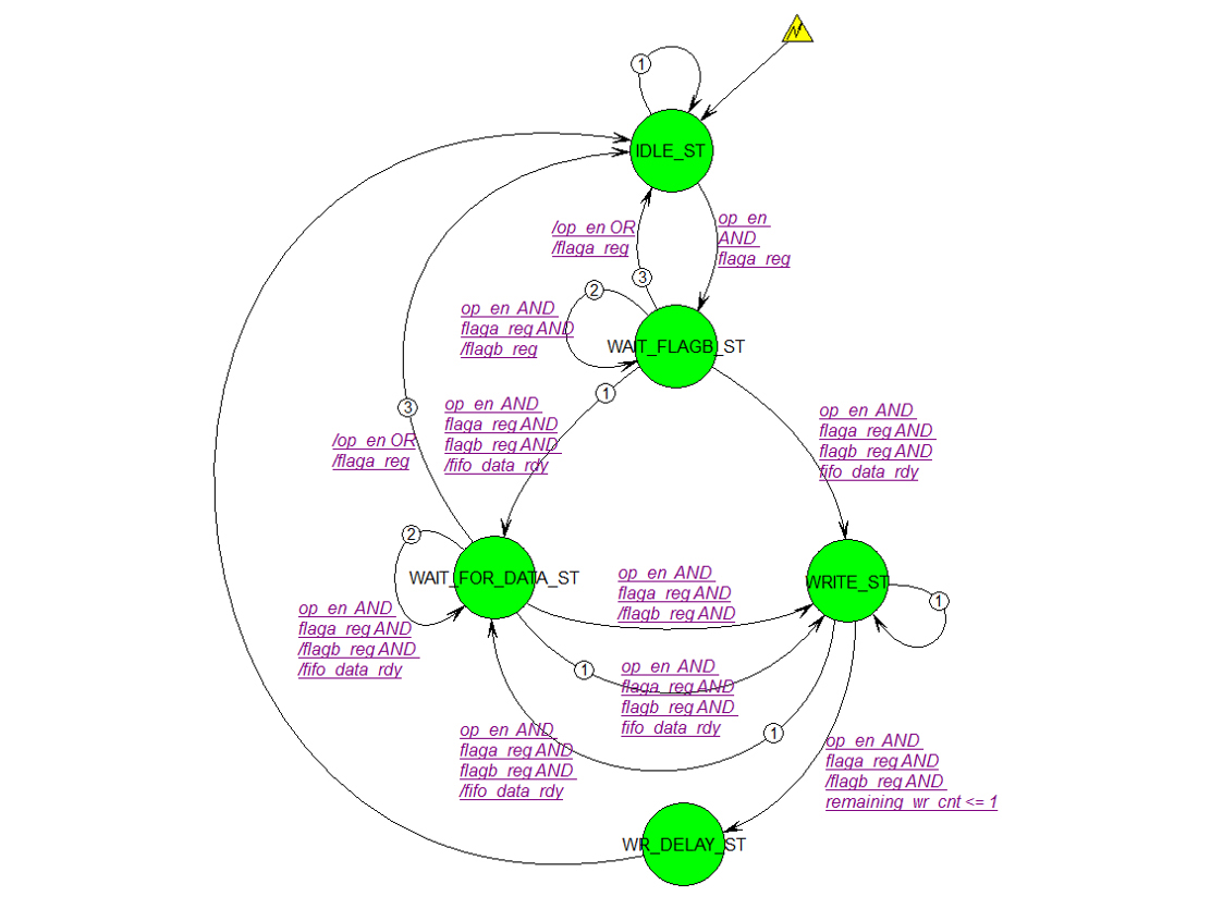
Figure 6-44: Slave FIFO interface state machine
- Confirmation
-
It looks like you're in the . If this is not your location, please select the correct region or country below.
You're headed to Hamamatsu Photonics website for US (English). If you want to view an other country's site, the optimized information will be provided by selecting options below.
In order to use this website comfortably, we use cookies. For cookie details please see our cookie policy.
- Cookie Policy
-
This website or its third-party tools use cookies, which are necessary to its functioning and required to achieve the purposes illustrated in this cookie policy. By closing the cookie warning banner, scrolling the page, clicking a link or continuing to browse otherwise, you agree to the use of cookies.
Hamamatsu uses cookies in order to enhance your experience on our website and ensure that our website functions.
You can visit this page at any time to learn more about cookies, get the most up to date information on how we use cookies and manage your cookie settings. We will not use cookies for any purpose other than the ones stated, but please note that we reserve the right to update our cookies.
1. What are cookies?
For modern websites to work according to visitor’s expectations, they need to collect certain basic information about visitors. To do this, a site will create small text files which are placed on visitor’s devices (computer or mobile) - these files are known as cookies when you access a website. Cookies are used in order to make websites function and work efficiently. Cookies are uniquely assigned to each visitor and can only be read by a web server in the domain that issued the cookie to the visitor. Cookies cannot be used to run programs or deliver viruses to a visitor’s device.
Cookies do various jobs which make the visitor’s experience of the internet much smoother and more interactive. For instance, cookies are used to remember the visitor’s preferences on sites they visit often, to remember language preference and to help navigate between pages more efficiently. Much, though not all, of the data collected is anonymous, though some of it is designed to detect browsing patterns and approximate geographical location to improve the visitor experience.
Certain type of cookies may require the data subject’s consent before storing them on the computer.
2. What are the different types of cookies?
This website uses two types of cookies:
- First party cookies. For our website, the first party cookies are controlled and maintained by Hamamatsu. No other parties have access to these cookies.
- Third party cookies. These cookies are implemented by organizations outside Hamamatsu. We do not have access to the data in these cookies, but we use these cookies to improve the overall website experience.
3. How do we use cookies?
This website uses cookies for following purposes:
- Certain cookies are necessary for our website to function. These are strictly necessary cookies and are required to enable website access, support navigation or provide relevant content. These cookies direct you to the correct region or country, and support security and ecommerce. Strictly necessary cookies also enforce your privacy preferences. Without these strictly necessary cookies, much of our website will not function.
- Analytics cookies are used to track website usage. This data enables us to improve our website usability, performance and website administration. In our analytics cookies, we do not store any personal identifying information.
- Functionality cookies. These are used to recognize you when you return to our website. This enables us to personalize our content for you, greet you by name and remember your preferences (for example, your choice of language or region).
- These cookies record your visit to our website, the pages you have visited and the links you have followed. We will use this information to make our website and the advertising displayed on it more relevant to your interests. We may also share this information with third parties for this purpose.
Cookies help us help you. Through the use of cookies, we learn what is important to our visitors and we develop and enhance website content and functionality to support your experience. Much of our website can be accessed if cookies are disabled, however certain website functions may not work. And, we believe your current and future visits will be enhanced if cookies are enabled.
4. Which cookies do we use?
There are two ways to manage cookie preferences.
- You can set your cookie preferences on your device or in your browser.
- You can set your cookie preferences at the website level.
If you don’t want to receive cookies, you can modify your browser so that it notifies you when cookies are sent to it or you can refuse cookies altogether. You can also delete cookies that have already been set.
If you wish to restrict or block web browser cookies which are set on your device then you can do this through your browser settings; the Help function within your browser should tell you how. Alternatively, you may wish to visit www.aboutcookies.org, which contains comprehensive information on how to do this on a wide variety of desktop browsers.
5. What are Internet tags and how do we use them with cookies?
Occasionally, we may use internet tags (also known as action tags, single-pixel GIFs, clear GIFs, invisible GIFs and 1-by-1 GIFs) at this site and may deploy these tags/cookies through a third-party advertising partner or a web analytical service partner which may be located and store the respective information (including your IP-address) in a foreign country. These tags/cookies are placed on both online advertisements that bring users to this site and on different pages of this site. We use this technology to measure the visitors' responses to our sites and the effectiveness of our advertising campaigns (including how many times a page is opened and which information is consulted) as well as to evaluate your use of this website. The third-party partner or the web analytical service partner may be able to collect data about visitors to our and other sites because of these internet tags/cookies, may compose reports regarding the website’s activity for us and may provide further services which are related to the use of the website and the internet. They may provide such information to other parties if there is a legal requirement that they do so, or if they hire the other parties to process information on their behalf.
If you would like more information about web tags and cookies associated with on-line advertising or to opt-out of third-party collection of this information, please visit the Network Advertising Initiative website http://www.networkadvertising.org.
6. Analytics and Advertisement Cookies
We use third-party cookies (such as Google Analytics) to track visitors on our website, to get reports about how visitors use the website and to inform, optimize and serve ads based on someone's past visits to our website.
You may opt-out of Google Analytics cookies by the websites provided by Google:
https://tools.google.com/dlpage/gaoptout?hl=en
As provided in this Privacy Policy (Article 5), you can learn more about opt-out cookies by the website provided by Network Advertising Initiative:
http://www.networkadvertising.org
We inform you that in such case you will not be able to wholly use all functions of our website.
Close