Application notes


Technical notes
Ask an engineer


Publications
United States (EN)
Select your region or country.
InGaAs linear sensor reference circuit design - Section 9
John Gilmore, Lu Cheng, Hamamatsu Corporation
Scott Hunt, Analog Devices, Inc.
December 15, 2018
Section 1: Introduction
Section 2: System description
Section 3: Analog devices sensor board
Section 4: FPGA/USB processor data path
Section 5: FPGA/USB processor control/status path
Section 6: FPGA design description
Section 7: USB sub-system
Section 8: PC software and IGAA driver library
Section 9: Test results
This technical note is divided into nine sections. To navigate to any section, use the hyperlinks above.
Section 9: Test Results
9A. Timing Operations and Analog I/O Signals
This is the timing diagram of the G9201~8 and G9211~4 sensors. The integration time is set by the Reset input pulse width. Each pixel is being read out every 8 clocks.
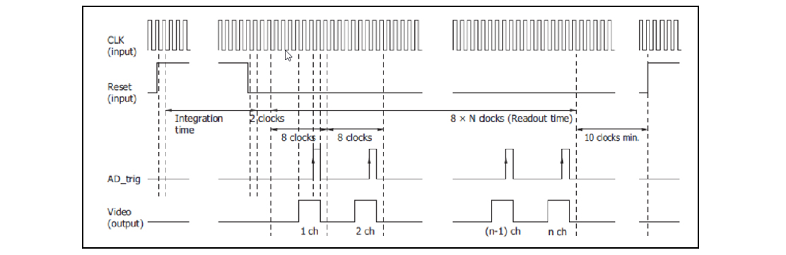
Figure 9-1: The G920x sensor timing diagram
In the software interface, the pixel format, readout mode, integration time, temperature, bias voltages, and the number of line data to be written can be defined.
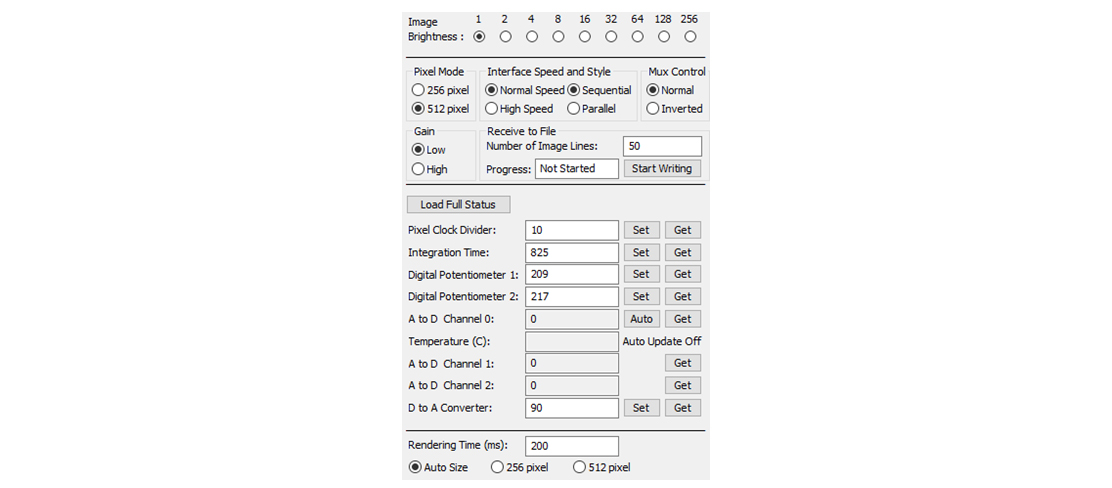
Figure 9-2: Parameter setting in the software interface
Pixel Number Select: 256 or 512.
For a 512-pixel array, there are two video output ports on the sensor chip: even and odd. Three readout modes are designed to read out from the sensor depending on the different multiplexer timing:
Multiplexer Timing (1) – Even/Odd simultaneous (parallel)
Multiplexer Timing (1a) – Non-Return to Zero (stagger)
Multiplexer Timing (2) – Clock burst with return to zero between pixel reads (bursts) – the same as C8062, the standard InGaAs multichannel detector head offered by Hamamatsu
The three different timing modes are tested, and the timing diagrams and test results are shown in Figures 9-3 to 9-18.
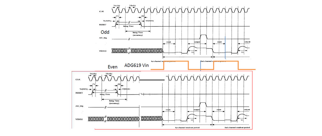
Figure 9-3: Timing diagram of MUX Timing (1) - Parallel clocking
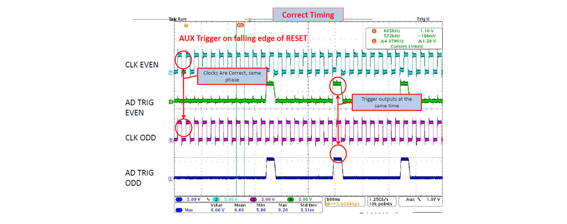
Figure 9-4: Test results of CLK and AD_Trig signals at MUX Timing (1)
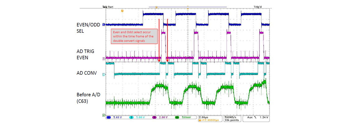
Figure 9-5: Test results of video output signal at MUX Timing (1)
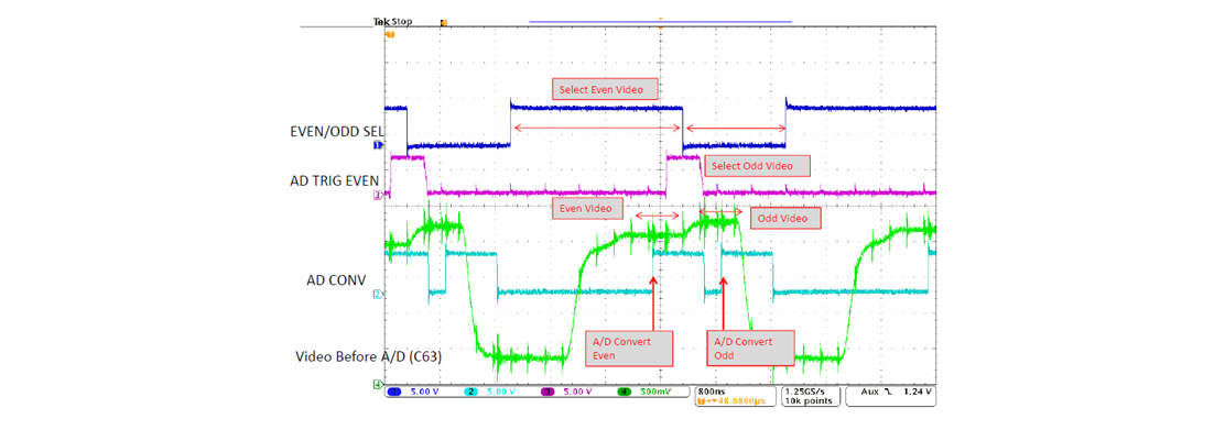
Figure 9-6: Test results of Even/Odd SEL and video output signals at MUX Timing (1)
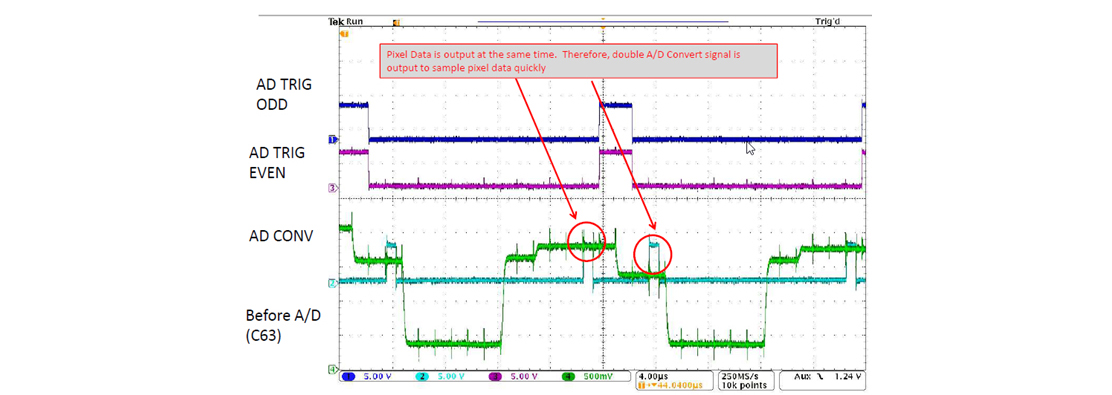
Figure 9-7: Test results of AD_CONV and video output signals at MUX Timing (1)
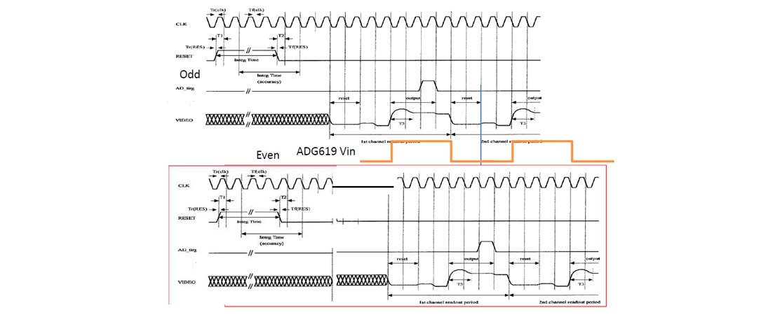
Figure 9-8: Timing diagram of MUX Timing (1a)
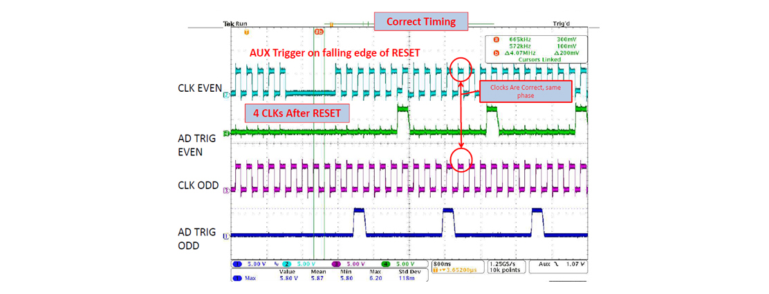
Figure 9-9: Test results of CLK and AD_Trig signals at MUX Timing (1a)
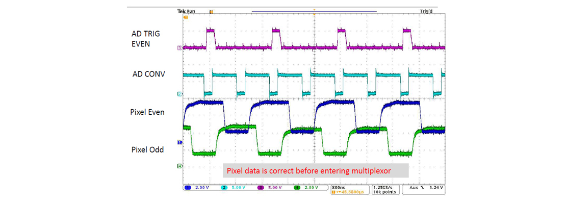
Figure 9-10: Test results of AD_CONV and video signals at MUX Timing (1a)
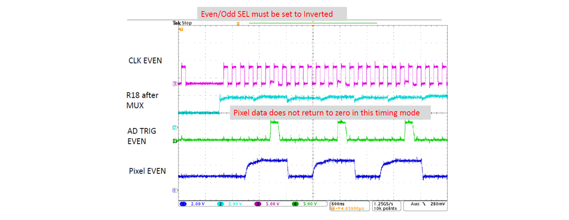
Figure 9-11: Test results of CLK and MUX output signals at MUX Timing (1a)
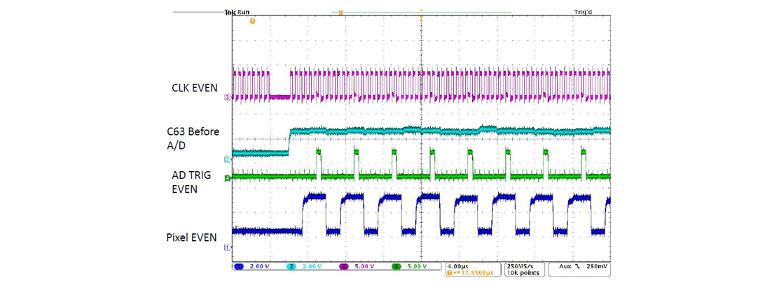
Figure 9-12: Test results of CLK, AD_Trig and video output signals at MUX Timing (1a)
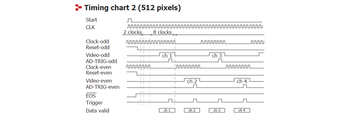
Figure 9-13: Timing diagram of MUX Timing (2)
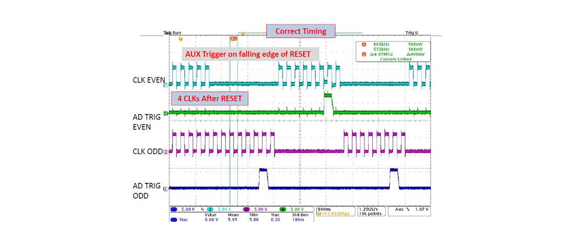
Figure 9-14: Test results of CLK and AD_Trig signals at MUX Timing (2)
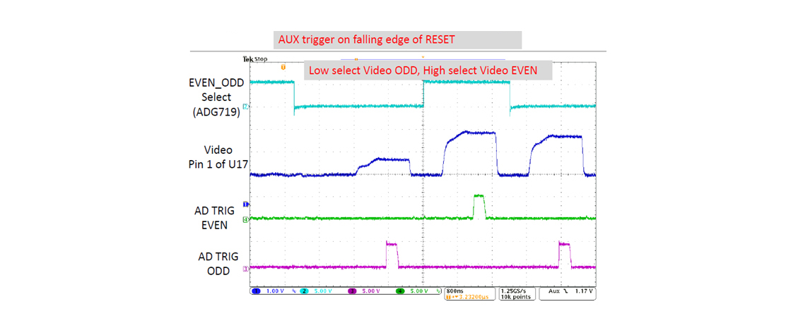
Figure 9-15: Test results of Even/Odd SEL and video output signals at MUX Timing (2)
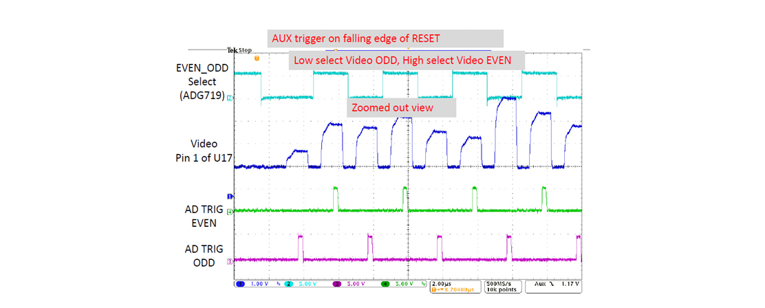
Figure 9-16: Zoom-out view of Figure 9-15
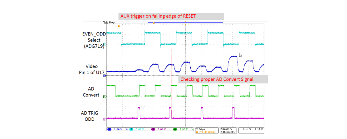
Figure 9-17: Test results of AD_CONV and video output signals at MUX Timing (2)
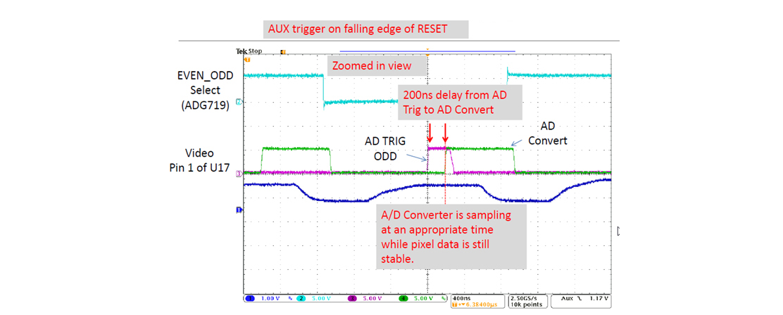
Figure 9-18: Zoom-in view of Figure 9-17
9B. Dark Stability
To verify the dark output is stable over time, indicating the InGaAs sensor cold-side temperature is stable at 0 deg. C., 600 scans are collected at 1 second integration time in the dark and the standard deviation is calculated for each pixel. Note: The level grouping is caused by Even/Odd CMOS ROIC variation. This is normal Even/Odd output pattern.
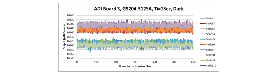
Figure 9-19: Dark measurement at 1 sec integration time
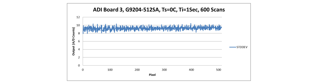
Figure 9-20: Standard deviation of 600 dark scans
9C. Noise
The readout noise was measured at 1 millisecond (msec) integration time.
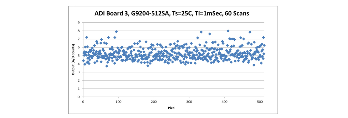
Figure 9-21: Readout measurement
Since the unity gain and the 5V reference voltage of ADC are used, one LSB represents 76.3µV. The readout noise is in the range of 300µV~600µV.
9D. Linearity
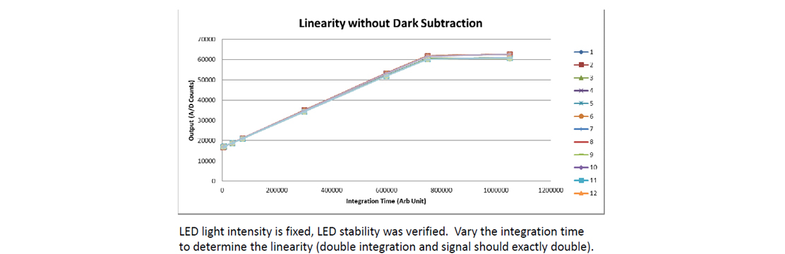
Figure 9-22: Linearity measurement with varying integration time
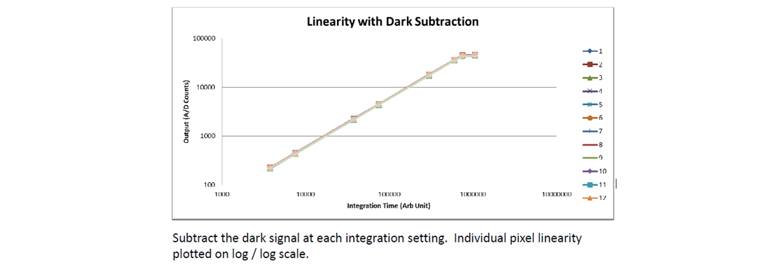
Figure 9-23: Linearity measurement with dark subtraction
- Confirmation
-
It looks like you're in the . If this is not your location, please select the correct region or country below.
You're headed to Hamamatsu Photonics website for US (English). If you want to view an other country's site, the optimized information will be provided by selecting options below.
In order to use this website comfortably, we use cookies. For cookie details please see our cookie policy.
- Cookie Policy
-
This website or its third-party tools use cookies, which are necessary to its functioning and required to achieve the purposes illustrated in this cookie policy. By closing the cookie warning banner, scrolling the page, clicking a link or continuing to browse otherwise, you agree to the use of cookies.
Hamamatsu uses cookies in order to enhance your experience on our website and ensure that our website functions.
You can visit this page at any time to learn more about cookies, get the most up to date information on how we use cookies and manage your cookie settings. We will not use cookies for any purpose other than the ones stated, but please note that we reserve the right to update our cookies.
1. What are cookies?
For modern websites to work according to visitor’s expectations, they need to collect certain basic information about visitors. To do this, a site will create small text files which are placed on visitor’s devices (computer or mobile) - these files are known as cookies when you access a website. Cookies are used in order to make websites function and work efficiently. Cookies are uniquely assigned to each visitor and can only be read by a web server in the domain that issued the cookie to the visitor. Cookies cannot be used to run programs or deliver viruses to a visitor’s device.
Cookies do various jobs which make the visitor’s experience of the internet much smoother and more interactive. For instance, cookies are used to remember the visitor’s preferences on sites they visit often, to remember language preference and to help navigate between pages more efficiently. Much, though not all, of the data collected is anonymous, though some of it is designed to detect browsing patterns and approximate geographical location to improve the visitor experience.
Certain type of cookies may require the data subject’s consent before storing them on the computer.
2. What are the different types of cookies?
This website uses two types of cookies:
- First party cookies. For our website, the first party cookies are controlled and maintained by Hamamatsu. No other parties have access to these cookies.
- Third party cookies. These cookies are implemented by organizations outside Hamamatsu. We do not have access to the data in these cookies, but we use these cookies to improve the overall website experience.
3. How do we use cookies?
This website uses cookies for following purposes:
- Certain cookies are necessary for our website to function. These are strictly necessary cookies and are required to enable website access, support navigation or provide relevant content. These cookies direct you to the correct region or country, and support security and ecommerce. Strictly necessary cookies also enforce your privacy preferences. Without these strictly necessary cookies, much of our website will not function.
- Analytics cookies are used to track website usage. This data enables us to improve our website usability, performance and website administration. In our analytics cookies, we do not store any personal identifying information.
- Functionality cookies. These are used to recognize you when you return to our website. This enables us to personalize our content for you, greet you by name and remember your preferences (for example, your choice of language or region).
- These cookies record your visit to our website, the pages you have visited and the links you have followed. We will use this information to make our website and the advertising displayed on it more relevant to your interests. We may also share this information with third parties for this purpose.
Cookies help us help you. Through the use of cookies, we learn what is important to our visitors and we develop and enhance website content and functionality to support your experience. Much of our website can be accessed if cookies are disabled, however certain website functions may not work. And, we believe your current and future visits will be enhanced if cookies are enabled.
4. Which cookies do we use?
There are two ways to manage cookie preferences.
- You can set your cookie preferences on your device or in your browser.
- You can set your cookie preferences at the website level.
If you don’t want to receive cookies, you can modify your browser so that it notifies you when cookies are sent to it or you can refuse cookies altogether. You can also delete cookies that have already been set.
If you wish to restrict or block web browser cookies which are set on your device then you can do this through your browser settings; the Help function within your browser should tell you how. Alternatively, you may wish to visit www.aboutcookies.org, which contains comprehensive information on how to do this on a wide variety of desktop browsers.
5. What are Internet tags and how do we use them with cookies?
Occasionally, we may use internet tags (also known as action tags, single-pixel GIFs, clear GIFs, invisible GIFs and 1-by-1 GIFs) at this site and may deploy these tags/cookies through a third-party advertising partner or a web analytical service partner which may be located and store the respective information (including your IP-address) in a foreign country. These tags/cookies are placed on both online advertisements that bring users to this site and on different pages of this site. We use this technology to measure the visitors' responses to our sites and the effectiveness of our advertising campaigns (including how many times a page is opened and which information is consulted) as well as to evaluate your use of this website. The third-party partner or the web analytical service partner may be able to collect data about visitors to our and other sites because of these internet tags/cookies, may compose reports regarding the website’s activity for us and may provide further services which are related to the use of the website and the internet. They may provide such information to other parties if there is a legal requirement that they do so, or if they hire the other parties to process information on their behalf.
If you would like more information about web tags and cookies associated with on-line advertising or to opt-out of third-party collection of this information, please visit the Network Advertising Initiative website http://www.networkadvertising.org.
6. Analytics and Advertisement Cookies
We use third-party cookies (such as Google Analytics) to track visitors on our website, to get reports about how visitors use the website and to inform, optimize and serve ads based on someone's past visits to our website.
You may opt-out of Google Analytics cookies by the websites provided by Google:
https://tools.google.com/dlpage/gaoptout?hl=en
As provided in this Privacy Policy (Article 5), you can learn more about opt-out cookies by the website provided by Network Advertising Initiative:
http://www.networkadvertising.org
We inform you that in such case you will not be able to wholly use all functions of our website.
Close