Application notes


Technical notes
Ask an engineer


Publications
United States (EN)
Select your region or country.
InGaAs linear sensor reference circuit design - Section 4
John Gilmore, Lu Cheng, Hamamatsu Corporation
Scott Hunt, Analog Devices, Inc.
December 15, 2018
Section 1: Introduction
Section 2: System description
Section 3: Analog devices sensor board
Section 4: FPGA/USB processor data path
Section 5: FPGA/USB processor control/status path
Section 6: FPGA design description
Section 7: USB sub-system
Section 8: PC software and IGAA driver library
Section 9: Test results
This technical note is divided into nine sections. To navigate to any section, use the hyperlinks above.
Section 4: FPGA/USB Processor Data Path
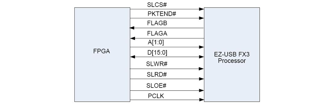
Figure 4-1: FPGA to EZ-USB FX3 interface
The pixel data is transferred between the FPGA and the USB processor using a 16-bit Synchronous Slave FIFO interface operating at 80MHz.
The data stream consists of 16-bit pixel word comprising 256 or 512 pixels per line.
The line-to-line separator consists of 2x 16-bit marker words:
Marker Word 1: 0xAAAA
Marker Word 2: 0x5555
The marker words appear in sequence: Marker Word 1, followed by Marker Word 2. The marker words are intended to serve the function equivalent to V-sync in video frames.
Note: There is no equivalent H-syncs as the frame is a single line.
4A. Interface Configuration
- Table 4-1 Data Path I/O Configuration
-
CYUSB3014-BZX Pin
Synchronous Slave FIFO Interface with 16-bit Data Bus
Interconnect Board
Net NameFPGA Pin
EZ-USB PWB
I/O VoltageDescription
Name
Location
Data Path
GPIO[17] K8 SLCS# CTL0 L1 VIO1 This is the chip select signal for the Slave FIFO interface. It must be asserted to access Slave FIFO. GPIO[18] K7 SLWR# CTL1 L4 VIO1 This is the write strobe for the Slave FIFO interface. It must be asserted for performing write transfers to Slave FIFO. GPIO[19] J7 SLOE# CTL2 M2 VIO1 This is the output enable signal. It causes the data bus of the Slave FIFO interface to be driven by FX3. It must be asserted for performing read transfers from Slave FIFO. GPIO[20] H7 SLRD# CTL3 L3 VIO1 This is the read strobe for the Slave FIFO interface. It must be asserted for performing read transfers from Slave FIFO. GPIO[21] G7 FLAGA CTL4 L18 VIO1 These are the FLAG outputs from FX3. The FLAGs indicate the availability of an FX3 socket.
FLAGA is configured as Current_thread_DMA_RDY.
FLAGB is configured as Current_thread_DMA_watermark.
GPIO[22] G6 FLAGB CTL5 L16 VIO1 GPIO[23] K6 FLAGC CTL6 P2 VIO1 GPIO[25] G5 FLAGD CTL8 T3 VIO1 GPIO[24] H8 PKTEND# CTL7 P1 VIO1 This signal is asserted to write a short packet or a zero length packet to Slave FIFO. GPIO[28] J5 A1 CTL11 G18 VIO1 This is the 2-bit address bus of Slave FIFO. GPIO[29] H5 A0 CTL12 K18 VIO1 GPIO[0] F10 DQ[0] DQ[0] H6 VIO1 This is the 16-bit data bus of Slave FIFO. GPIO[1] F9 DQ[1] DQ[1] D3 VIO1 GPIO[2] F7 DQ[2] DQ[2] M5 VIO1 GPIO[3] G10 DQ[3] DQ[3] L6 VIO1 GPIO[4] G9 DQ[4] DQ[4] T1 VIO1 GPIO[5] F8 DQ[5] DQ[5] M3 VIO1 GPIO[6] H10 DQ[6] DQ[6] N7 VIO1 GPIO[7] H9 DQ[7] DQ[7] T2 VIO1 GPIO[8] J10 DQ[8] DQ[8] N8 VIO1 GPIO[9] J9 DQ[9] DQ[9] H15 VIO1 GPIO[10] K11 DQ[10] DQ[10] J13 VIO1 GPIO[11] L10 DQ[11] DQ[11] H16 VIO1 GPIO[12] K10 DQ[12] DQ[12] N10 VIO1 GPIO[13] K9 DQ[13] DQ[13] N16 VIO1 GPIO[14] J8 DQ[14] DQ[14] N11 VIO1 GPIO[15] G8 DQ[15] DQ[15] N15 VIO1 GPIO[16] J6 PCLK HSMC_CLKOUT_p2 U18 VIO1 Slave Interface clock 80 MHz.
Note: Jumper on interconnect board from J3.44 to J2.155 needed
4B. EZ-USB Development Board Configuration
- Table 4-2 EZ-USB Development Board Configuration
-
PWB Reference Designator Configuration (Jumper/Switch Setting) J40 Open J42 2-3 shorted J45 2-3 shorted J47 Open J50 Open J52 2-3 shorted J53 1-3 shorted J72 1-2 shorted J74 Open J98 Open J97 2-3 shorted J96 2-3 shorted J100 1-2 shorted J101 2-3 shorted J102 2-3 shorted J104 1-2 shorted J103 1-2 shorted J125 1-2 shorted J134 3-6 shorted J135 2-4 shorted J136 2-5 shorted J143 2-5 shorted J144 2-5 shorted J145 2-5 shorted J146 2-5 shorted J156 Open SW25 1 = OFF
2 = OFF
3 = ON
4 = ONSW40 1 = ON
2 = ON
3 = ON
4 = ON
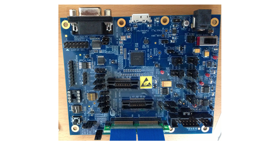
Figure 4-2: Cypress EZ-USB development board configuration
4C. FPGA/USB Processor Interface
The USB processor configures the FPGA control registers via I2C interface as described in Section 5. Once the desired configuration parameters have been set, the USB processor sets Reg_01 bits (7:6) = “11”, enabling the sensor control and the Slave FIFO operation.
The USB processor can disable the sensor control and/or Slave FIFO operation at any time in order to re-configure the control registers.
- Confirmation
-
It looks like you're in the . If this is not your location, please select the correct region or country below.
You're headed to Hamamatsu Photonics website for US (English). If you want to view an other country's site, the optimized information will be provided by selecting options below.
In order to use this website comfortably, we use cookies. For cookie details please see our cookie policy.
- Cookie Policy
-
This website or its third-party tools use cookies, which are necessary to its functioning and required to achieve the purposes illustrated in this cookie policy. By closing the cookie warning banner, scrolling the page, clicking a link or continuing to browse otherwise, you agree to the use of cookies.
Hamamatsu uses cookies in order to enhance your experience on our website and ensure that our website functions.
You can visit this page at any time to learn more about cookies, get the most up to date information on how we use cookies and manage your cookie settings. We will not use cookies for any purpose other than the ones stated, but please note that we reserve the right to update our cookies.
1. What are cookies?
For modern websites to work according to visitor’s expectations, they need to collect certain basic information about visitors. To do this, a site will create small text files which are placed on visitor’s devices (computer or mobile) - these files are known as cookies when you access a website. Cookies are used in order to make websites function and work efficiently. Cookies are uniquely assigned to each visitor and can only be read by a web server in the domain that issued the cookie to the visitor. Cookies cannot be used to run programs or deliver viruses to a visitor’s device.
Cookies do various jobs which make the visitor’s experience of the internet much smoother and more interactive. For instance, cookies are used to remember the visitor’s preferences on sites they visit often, to remember language preference and to help navigate between pages more efficiently. Much, though not all, of the data collected is anonymous, though some of it is designed to detect browsing patterns and approximate geographical location to improve the visitor experience.
Certain type of cookies may require the data subject’s consent before storing them on the computer.
2. What are the different types of cookies?
This website uses two types of cookies:
- First party cookies. For our website, the first party cookies are controlled and maintained by Hamamatsu. No other parties have access to these cookies.
- Third party cookies. These cookies are implemented by organizations outside Hamamatsu. We do not have access to the data in these cookies, but we use these cookies to improve the overall website experience.
3. How do we use cookies?
This website uses cookies for following purposes:
- Certain cookies are necessary for our website to function. These are strictly necessary cookies and are required to enable website access, support navigation or provide relevant content. These cookies direct you to the correct region or country, and support security and ecommerce. Strictly necessary cookies also enforce your privacy preferences. Without these strictly necessary cookies, much of our website will not function.
- Analytics cookies are used to track website usage. This data enables us to improve our website usability, performance and website administration. In our analytics cookies, we do not store any personal identifying information.
- Functionality cookies. These are used to recognize you when you return to our website. This enables us to personalize our content for you, greet you by name and remember your preferences (for example, your choice of language or region).
- These cookies record your visit to our website, the pages you have visited and the links you have followed. We will use this information to make our website and the advertising displayed on it more relevant to your interests. We may also share this information with third parties for this purpose.
Cookies help us help you. Through the use of cookies, we learn what is important to our visitors and we develop and enhance website content and functionality to support your experience. Much of our website can be accessed if cookies are disabled, however certain website functions may not work. And, we believe your current and future visits will be enhanced if cookies are enabled.
4. Which cookies do we use?
There are two ways to manage cookie preferences.
- You can set your cookie preferences on your device or in your browser.
- You can set your cookie preferences at the website level.
If you don’t want to receive cookies, you can modify your browser so that it notifies you when cookies are sent to it or you can refuse cookies altogether. You can also delete cookies that have already been set.
If you wish to restrict or block web browser cookies which are set on your device then you can do this through your browser settings; the Help function within your browser should tell you how. Alternatively, you may wish to visit www.aboutcookies.org, which contains comprehensive information on how to do this on a wide variety of desktop browsers.
5. What are Internet tags and how do we use them with cookies?
Occasionally, we may use internet tags (also known as action tags, single-pixel GIFs, clear GIFs, invisible GIFs and 1-by-1 GIFs) at this site and may deploy these tags/cookies through a third-party advertising partner or a web analytical service partner which may be located and store the respective information (including your IP-address) in a foreign country. These tags/cookies are placed on both online advertisements that bring users to this site and on different pages of this site. We use this technology to measure the visitors' responses to our sites and the effectiveness of our advertising campaigns (including how many times a page is opened and which information is consulted) as well as to evaluate your use of this website. The third-party partner or the web analytical service partner may be able to collect data about visitors to our and other sites because of these internet tags/cookies, may compose reports regarding the website’s activity for us and may provide further services which are related to the use of the website and the internet. They may provide such information to other parties if there is a legal requirement that they do so, or if they hire the other parties to process information on their behalf.
If you would like more information about web tags and cookies associated with on-line advertising or to opt-out of third-party collection of this information, please visit the Network Advertising Initiative website http://www.networkadvertising.org.
6. Analytics and Advertisement Cookies
We use third-party cookies (such as Google Analytics) to track visitors on our website, to get reports about how visitors use the website and to inform, optimize and serve ads based on someone's past visits to our website.
You may opt-out of Google Analytics cookies by the websites provided by Google:
https://tools.google.com/dlpage/gaoptout?hl=en
As provided in this Privacy Policy (Article 5), you can learn more about opt-out cookies by the website provided by Network Advertising Initiative:
http://www.networkadvertising.org
We inform you that in such case you will not be able to wholly use all functions of our website.
Close