Application notes
Technical notes
Ask an engineer
Publications
United States (EN)
Select your region or country.
Image sensors product selection
Ardavan Ghassemi, Hamamatsu Corporation
February 22, 2017
Table of Contents
Section 1. Image sensor performance parameter
1.1 Signal
1.2 Noise
1.3 Signal-to-noise ratio
1.4 Fixed-pattern noise
1.5 Dynamic range
1.6 Linearity
1.7 Contrast and spatial resolution
1.8 Timing operations
Section 2. Case studies of assessing image sensor performance
2.1 Line/frame rates
2.2 MOS image sensors
2.3 CCD image sensors
2.4 InGaAs image sensors
2.5 SNR calculations
In this technical note, an overview of generalized methods for selection of image sensor products (NMOS, CMOS, CCD, InGaAs) for a broad range of applications is provided. A primary objective has been to describe methods that could be used for any application as long as certain basic pieces of information are available about the target application; these methods could be used for product selection consistently despite the application’s peculiarities.
However, it is important to note that the methods described in this technical note are meant to serve as preliminary general guidelines (so-called ‘back-of-the-envelope’ calculations); they are intended to serve as early indicators of what product(s) to begin considering for evaluation. As the technical considerations advance, these methods would not substitute for proper simulation and experimentation under the specific conditions of the intended application.
The content of this technical note assumes a working knowledge of characteristics and operation principles of image sensors. To gain that knowledge, please review Hamamatsu’s Opto-Semiconductor Handbook, FFT-CCD Technical Note, TDI-CCD Technical Note, and Resistive-Gate CCD Technical Note. This technical note consists of two main sections; the first section provides an overview of methods to assess image sensor performance, and the second describes how to put those methods to use.
Section 1. Image sensor performance parameters
Each and every application that involves detection of light (regardless of its source: laser, LED, lamp, scintillation, different luminescence effects, etc.) can be defined and characterized by the following parameters:
1.1 Signal
An optical application’s input signal level is simply the amount of light that is to be detected or measured. In quantifying the amount of input signal present, the dimension or unit of measurement is essential for making proper calculations.
The two dimensions that could be used by the methods described in this technical note are watts [W] and number of photons. Note that the former is normalized to time while the latter is not (although it could be in addition to both being normalized to illumination area).
A signal level expressed in either of these units can be converted to the other by the following formula:
Equation 1.1a
Where:
T = light signal exposure time for one measurement.
There are other units (lm, lx, etc.) used to express the amount of illumination, but those units require tabulated reference data or complex calculations for their proper use, and hence, they are not discussed in this technical note as they exceed its intended scope.
Input light signal of a particular wavelength (λ) can be converted to output signal per channel (pixel) of an image sensor by the following relationship:
Equation 1.1b
Where:
Sdark = the pixel output charge during the measurement that is not generated as a result of the photoelectric effect
M = any internal avalanche gain
CCE = charge collection efficiency
CTE = charge transfer efficiency
CCE ~1 and CCT ~1 are typically attained in modern scientific-grade image sensors.
Amongst various types of image sensors, the vast majority have unity gain with the exception being electron-multiplying CCDs. (Electron-bombardment CCDs also have a gain mechanism, but it is external to the CCD.)
1.2 Noise
The intrinsic uncertainty or random fluctuation in a signal that is to be measured is noise. For an optical signal, that uncertainty or noise is characterized by constructing a histogram (a so-called pulse height distribution or PHD) of incidents of detected light pulses with varying heights (i.e., containing different counts of photons); the resulting histogram could be closely fitted into a profile similar to that of a Poisson probability distribution. That leads us to conclude that noise characteristics of a photon signal can be modeled by the following Poisson probability distribution function and its corresponding mean (μ) and standard deviation (σ):
Equation 1.2
To model the detection of light using the above probability model, the standard deviation is considered to be a measure of randomness or uncertainty (i.e., noise) of the Poisson random variable (i.e., photon signal), and the mean is the expected value of the signal. In other words, intrinsic noise of a light signal is described by the square root of its mean. A photodetector’s dark output also has a Poisson probability distribution. A noise whose random behavior can be characterized by a Poisson distribution is often referred to as “shot” noise.
In Eq. 1.1b, note the emphasis we placed on the dark output being concurrent with the measurement itself. Bear in mind that dark (or background) subtraction does not reduce dark shot noise but actually increases it, since this common correction technique does not utilize the dark signal that affects the measurement. It instead relies on dark output data that are obtained in close timing proximity to (optimally so if possible) the measurement (but not during it) and are hence different (albeit perhaps slightly) from the dark output present in the measurement.
If X and Y are dark signal in an object’s image and dark signal in a dark image, respectively, and are as such independent random variables, considering that , we have the following relationship between their standard deviations: in which X–Y is the result of dark subtraction. Thus, dark subtraction increases dark shot noise (despite diminishing electronic offset). Keep in mind that a most effective way to diminish dark shot noise is by suppressing thermal carrier generation through cooling.
1.3 Signal-to-noise ratio (SNR)
As its name suggests, it is the ratio of signal to noise as calculated for a detector’s output. In light detection applications with unity gain, it is fundamentally defined by:
Equation 1.3a
Where:
nphoton shot = photon shot noise
ndark shot = dark shot noise
nreadout = readout noise at the applicable pixel readout frequency
Considering their Poisson probability distributions, photon shot noise and dark shot noise can be obtained as square roots of counts of photoelectrons and dark electrons, and thus, Eq. 1.3a can be simplified to:
Equation 1.3b
However, if background light is present in addition to the certain wavelength (λi) of the light signal, SNR must be calculated more comprehensively as:
Equation 1.3c
In the case of EM-CCD, which has an internal avalanche gain mechanism, SNR is obtained by
Equation 1.3d
in which F is excess noise factor, which is gain-dependent (but ~ 1.4 is a reasonable generalized estimation). Considering that Hamamatsu does not manufacture EM-CCDs at the time of this writing, this type of image sensor is not discussed further in this technical note.
It is noteworthy to add that when a CCD is operated in time-delay integration (TDI) mode for imaging of moving objects or in line-binning mode for spectrometry, SNR is improved by a factor up to the square root of the number of TDI or line-binning charge transfers.
1.4 Fixed-pattern noise (FPN)
FPN is a spatial variation in an image sensor’s output in response to uniform illumination. FPN is caused by a combination of variations in photosensitivity of an image sensor’s pixels (an effect known as photo-response non-uniformity or PRNU and commonly characterized by the ratio of an image’s standard deviation of pixel output values to their mean) and differences in gain and offset amongst an image sensor’s multiple readout amplifiers (whether those of active-pixel CMOS sensors or multiport CCD and passive-pixel CMOS sensors). The variations and differences in question manifest themselves in a relatively fixed spatial pattern.
For reducing FPN in images obtained from any readout mode, flat-field correction is an effective technique that can be performed by the following equation:
Equation 1.4
in which Iffc is the flat-field-corrected image, Iobj is the image to be corrected (i.e., image of the desired object), Idark is a background image with no illumination, Iff is a bright-field image with uniform full illumination of the image sensor’s active area (i.e., no object in the imager’s field-of-view), and C is the mean value of all pixels in Iff-Idark.
All of these images must be obtained at the same integration time and image sensor temperature. The flat-field correction’s efficacy can be improved if the images used are each averaged over several frames (up to 10-20 frames but no need for more due to diminishing improvement).
1.5 Dynamic range (DR)
DR is typically expressed as a ratio between two levels of the input signal. One level (as numerator of the ratio) is the amount of accumulated (dark and photoelectron) charge at which the image sensor’s output saturates. The other (denominator of the ratio) is the image sensor’s readout noise as its limiting noise floor. Key use of DR is in selecting a suitable ADC for digitizing the output of an image sensor: ideally, the ADC’s bit range must be equivalent (by a log2 relationship) to the image sensor’s DR. Practically, that is not a convenient equivalence to attain, however, so an extra bit(s) is often present. Nonetheless, for economic (i.e., component cost) or marketing reasons, an ADC with a much wider bit range than necessary might be adopted by the camera designer; that wider bit range would yield no technical benefit.
It is noteworthy to add here that the digitization process itself introduces a further degree of uncertainty or noise to the digitized value of a measured signal due to the discrete quantized nature of the process. That digitization noise can be approximated as ndigitization ~ 0.3K in which K is the ADC’s conversion factor [e-/LSB].
To put the effect of digitization noise on SNR in perspective, we optimally define K = nreadout as discussed above. Consequently, we have: ndigitization=0.3 x nreadout. Calculating the net effect of digitization and readout noises together, we have:
Equation 1.5
Thus, ndigitization is commonly excluded from SNR calculations.
Additionally, the amplifier gain or conversion factor [V/e-] must ideally be set such that the image sensor’s min. output (i.e., readout noise) is converted by the ADC’s conversion factor [LSB/V or ADU/V] to <1 ADU or 0. However, considering that readout noise randomly fluctuates and also varies with pixel readout rate, it is sometimes preferable for the ADC to be biased with a conservative offset, and thus, some pixels in a digital image could have min. values larger than 0.
It is also noteworthy to add that the output amplifier's rail voltage must be such that it allows for the image sensor's output range to be converted to within the ADC's input voltage range.
1.6 Linearity
The extent to which the output of an image sensor has a linear relationship with its input (as defined by f(x) = b.x + c in which b and c are real constants) is the measure of the image sensor’s linearity and is fundamentally defined by:
Equation 1.6a
in which A is signal amplitude and t represents passage of time. If the ratio of the 2 relative changes is < 1, nonlinearity exists.
For practical purposes, nonlinearity is typically of greater interest than linearity itself:
Equation 1.6b
Since image sensor response is theoretically linear (within the constraints of SNR > 1 and up to saturation), linearity can be practically obtained by:
Equation 1.6c
For linearity measurement in a practical setting, measurement data are obtained by varying an image sensor’s integration time and recording its real output in response to illumination from a stable light source. The ideal output is then linearly extrapolated from a measurement in which the image sensor’s real output is at or around half of saturation; ideal response is constructed by multiplying that real output (closest to half of saturation) by the ratio of its integration time to integration times of other real output data points.
A common misconception is that an image sensor’s output is linear over the full range of its DR between the readout noise floor and the output saturation level. However, image sensors can exhibit significant nonlinearity at very low signal levels (albeit over the readout noise floor) and at very high signal levels (although lower than the output saturation level).
Due to variations in pixel characteristics, such nonlinearities often manifest themselves locally. Thus, it is important to avoid considering suitability of an image sensor product for a particular application based on the product’s DR alone and instead rely on SNR calculations as a first step followed by actual linearity measurements for verification.
1.7 Contrast and spatial resolution
Image sensor pixel size and fill-factor, photosensitivity, and noise characteristics significantly contribute to differences in imaging contrast and resolution, which are related factors that represent how imaging SNR changes as finer and finer features are imaged; they are parameterized by contrast transfer function (CTF) and modulation transfer function (MTF).
Since measuring SNR as a function of spatial frequency is quite complex (due to its cardinal sinusoidal nature), simpler measurement definitions are usually utilized in practice instead. To measure CTF and MTF for an image sensor, a line-pair gauge of sequential square-wave spatial frequencies is imaged by the image sensor in question. By sequential spatial frequencies, we mean dark and bright (opaque and transparent) line pairs of varying feature size; frequency in this sense is measured in the unit of line pairs per mm [lp/mm]. For a spatial frequency f, CTF and MTF are defined by:
Equation 1.7a
Equation 1.7b
in which f0 is the frequency of a line pair whose feature size is many times (≥10) larger than that of the image sensor’s pixel and A is image signal amplitude. It is noteworthy to add that images used in calculations of CTF and MTF should be flat-field corrected for accurate results. Furthermore, any optical magnification should be taken into account in objective product performance assessment and comparison.
1.8 Timing operations
The period of time during which an image sensor forms and outputs an image consists of two phases: integration time and readout time. Integration is that portion of an image sensor’s operation cycle during which photocurrent is intended to be integrated.
The integrated char ge is then read out during readout time (as the name suggests); although, charge from dark current continues to be generated and added to the signal during readout. Another timing term is exposure time, which is that portion of integration time during which the image sensor is exposed to the light signal. For simplicity, in this technical note, we assume that integration time is set equal to the full duration of signal exposure, which is most often the case.
An applicable image sensor’s timing order of integration and readout operations constitutes whether that image sensor is designed to operate in global or rolling shutter modes: in the former, charge integration is performed in all pixels during the same time window, and then the integrated charges of all pixels are rapidly transferred to opaquely coated storage pixels (in the case of a frame-transfer CCD) or interline gates (in the case of an interline CCD) in order to be read out. This scheme enables imaging of fast-occurring events (such as rapid movement of an object) with little or no image smear.
Alternatively, 3-transistor NMOS/CMOS image sensors operate in the electronic rolling shutter mode in which pixel integration times are shifted in time by a certain overlap or delay in the order by which the pixels are read.
To explain better, in an array of N pixels, when pixel i is read and reset, its next integration time begins (considering that a pixel’s integration time is the duration of time between two consecutive readouts of it) and then pixel i+1 is read and begins to integrate, so integration time of pixel i+1 follows that of pixel i by a certain delay. In fact, integration times of all pixels (1, 2, 3, … , i–2, i–1, i, i+1, i+2, … , N) take place in serial order with a delay in between integrations of each consecutive pair of pixels between 1 and N. In that sense, one can think of the readout operation in the rolling shutter mode as a domino effect propagating through the matrix of pixel rows and columns in consecutive order.
It is important to note that rolling shutter mode is suitable for imaging static scenes (a still object or a fixed spectral pattern) or under illumination from a pulsed light source (of known pulse rate or as synchronized by a trigger signal to avoid light exposure during readout); image sensors operating in rolling shutter mode must be read out in synchronization with a mechanical shutter in order to avoid image distortion in imaging moving objects.
In selecting a suitable image sensor for spectroscopy, we often face the challenge that the required integration time for a weak wavelength is unknown. To overcome that, we use Eq. 1.8 to calculate how long an image sensor must be integrated in order to yield the desired SNR and assess whether that length of integration is practical and realistic or not (for instance, would it lead to output saturation for stronger wavelengths?).
Equation 1.8
Converting the above relationship to a quadratic equation and solving for Tintegration (as the unknown variable) would yield the integration time in question. In the above equation, note that Sinput should be in unit of [photons/s] and Sdark should be in unit of [electrons/s] in order to accommodate multiplication by time. We will discuss how to calculate Treadout in Section 2.
Section 2. Case studies of assessing image sensor performance
2.1 Line/frame rates
For an image sensor product, a max. pixel readout rate is typically specified; that is the fastest rate at which individual pixels can be read out during a single readout operation. However, that rate does not pertain to the rate at which the sensor can perform measurements (i.e., take images) consecutively.
Considering that an image sensor is a serial-readout multi-channel detector in which data measured by detector channels (pixels) must be read out in a serial order before the next set of measured data can be accessed, pixel rate only constitutes a portion of how frequently an image sensor can repeat measurements and produce images.
Thus, depending on the image format by which an image sensor is read, its line rate or frame rate is of far greater significance to the intended application than its pixel readout rate alone. In the following sections, we will discuss how to calculate line and frame rates for various types of image sensors that Hamamatsu manufactures.
Please bear in mind that a duty cycle of 50% is presumed for applicable clock signals in the following calculations for simplicity. Please also keep in mind that the following calculations are purely theoretical and simply serve as guides in preliminary technical considerations; in practice, clock signal rates and timing values are adopted by camera developers based on experimental studies of signal integrity, waveform deterioration, and noise effects.
Please also note that different calculations would apply to readout modes of other types of image sensors like 4- or 5-transistor “scientific” CMOS and frame-transfer and interline CCDs, but since Hamamatsu does not manufacture such products at the time of this writing, those are not discussed.
Now, let’s perform case studies of line and/or frame rates of various Hamamatsu image sensor products.
2.2 MOS image sensors
Hamamatsu’s 3-transistor linear NMOS and CMOS image sensors can be categorized as current-output and voltage-output types. For reading out the former type, the user must implement a charge amplifier circuitry while the latter type has a built-in charge amplifier. However, timing operations of both types are the same.
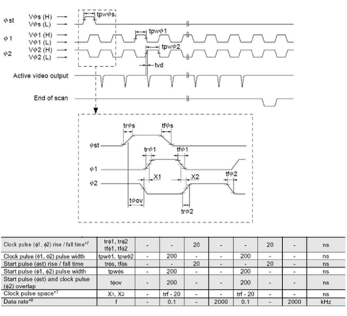
Figure 1. Typical timing diagram of an NMOS/CMOS linear image sensor (LIS) or photodiode array (PDA).
Table 1. Typical timing parameter of an NMOS/CMOS LIS or PDA.
| Clock pulse (Φ1,Φ2) rise/fall time | trΦ1, trΦ2 tfΦ1, tfΦ2 |
– | – | 20 | – | – | 20 | – | ns |
| Clock pulse (Φ1,Φ2) pulse width | tpwΦ1, tpwΦ2 | – | 200 | – | – | 200 | – | – | ns |
| Start pulse (Φst) rise/fall time | trΦs, tfΦs | – | – | 20 | – | – | 20 | – | ns |
| Start pulse (Φ1, Φ2) pulse width | tpwΦs | – | 200 | – | – | 200 | – | – | ns |
| Start pulse (Φst) and clock pulse (Φ2) overlap | tΦov | – | 200 | – | – | 200 | – | – | ns |
| Clock pulse space | X1,X2 | – | trf-20 | – | – | trf-20 | – | – | ns |
| Data rate | f | – | 0.1 | – | 2000 | 0.1 | – | 2000 | kHz |
About the above diagram and parameters, remember the following key points:
- CLK is an input clock signal that is fed to the sensor’s shift register. Frequency of this signal or f(CLK) is linearly proportional to the sensor’s pixel readout rate (also referred to as data rate); as an input signal, CLK is used to set the pixel readout rate of the LIS.
- The sensor’s integration time is the period of the ST (Start) input signal. Since these MOS image sensors operate in the rolling shutter mode, the sensor’s line rate is thus the inverse of the period of the ST signal.
Therefore, based on the above timing diagram, the min. integration can be calculated as:
Equation 2.2
in which is the min. period of ST and Npixel is total pixel count (not just count of effective pixels). Consequently, max. full line rate becomes .
Now, let’s try to calculate max. full line rates of a couple of sensors in this category. As a current-output NMOS PDA, we pick S3903-1024Q, which has min. and Npixel = 1024, and thus, we get a min. integration time of 409.6μs and a max. line rate of ~2.44KHz as a result. As a voltage-output NMOS LIS, we pick S3923-1024Q, which also has min. along with the same total pixel count, and hence, we get the same min. integration time and max. line rate.
As you review their datasheets, you will notice that min. integration time (and hence indirectly max. full line rate) has been indicated in datasheets of CMOS LIS products. For example, in the case of S9226 series (voltage-output type), min. ST period has been defined as while in the case of S10121 to S10124 series (current-output type) or S8377/8 series (voltage-output type), min. ST period is .
It is noteworthy that in applications that require higher line rates than what a particular LIS can nominally accommodate and in which just a fraction of the sensor’s pixels’ data is needed, it is possible to re-input the ST signal after the desired portion of pixels has been read out in order to initiate a new scan and integration period. However, doing so continually would eventually saturate and overflow the unread pixels, triggering the sensor’s anti-blooming mechanism. This scenario could be avoided after several such premature ST inputs by using the sensor’s ALL-RESET function (when available) to reset and drain all pixels, including the unread ones. One does so by bringing the sensor’s saturation control gate to a “High” level for a sacrificial duration of time (≥5μs in the case of S3902/3 and S3922/3 series).
2.3 CCD image sensors
Hamamatsu mainly manufactures 2D full-frame transfer or FFT-CCDs in 2-phase and 3-phase categories. Phase in this instance refers to how many vertical clock signals with corresponding phase differences ( in the case of 2-phase CCD and in the case of 3-phase CCD) are used to perform a charge transfer operation from a pixel row to the next. FFT-CCDs operate in a progressive-scan mode that has been extensively described in Hamamatsu’s FFT-CCD Technical Note. Without synchronization of readout operation with a mechanical shutter, this scan mode is solely suitable for imaging still objects using a strobe light source (of known frequency or as synchronized by a trigger signal to avoid illumination during readout) or measuring fixed spectral patterns; otherwise, severe image smear will occur.
2.3.1 2-Phase CCD
Most Hamamatsu CCDs are in this category and can operate as such due to one-directional dopant barriers between each two pixel rows; these barriers should not be confused with channel stops between pixel columns. Specialized for spectroscopy, these Hamamatsu CCDs are typically operated in line-binning mode, but as an intellectual exercise, we will also address those less common cases in which they are operated in area-readout mode.
Line-binning mode
Line binning is a common operation scheme to boost SNR in spectroscopic applications. In line binning, integrated charges in CCD pixels on one vertical column are binned together in the horizontal register before being clocked out of the register for readout. This technique is suitable for spectrometry since spectral bands of interest can be dispersed vertically along CCD pixel columns (and horizontally across pixel rows). To begin, please see the timing parameters and diagram of a typical FFT-CCD (S7030/S7031 series of back-illuminated CCDs in this case) in line-binning operation mode below.
Table 2. Timing parameters of FFT-CCD (S7030/S7031 series)
| Parameter | Symbol | Min. | Typ. | Max. | Unit | |
|---|---|---|---|---|---|---|
| P1V, P2V, TG | Pulse width S703*-0906 | Tpwv | 1.5 | 2 | - | μs |
| Pulse width S703*-0907/-1006 | Tpwv | 3 | 4 | - | μs | |
| Pulse width S703*-1007 | Tpwv | 6 | 8 | - | μs | |
| Rise and fall time | Tprv,Tpfv | 10 | - | - | ns | |
| P1H, P2H | Pulse width | Tpwh | 500 | 2000 | - | ns |
| Rise and fall time | Tprh,Tpfh | 10 | - | - | ns | |
| Duty ratio | - | - | 50 | - | % | |
| SG | Pulse width | Tpws | 500 | 2000 | - | ns |
| Rise and fall time | Tprs, Tpfs | 10 | - | - | ns | |
| Duty ratio | - | - | 50 | - | % | |
| RG | Pulse width | Tpwr | 100 | - | - | ns |
| Rise and fall time | Tprr, Tpfr | 5 | - | - | ns | |
| TG-P1H | Overlap time | Tovr | 3 | - | - | μs |
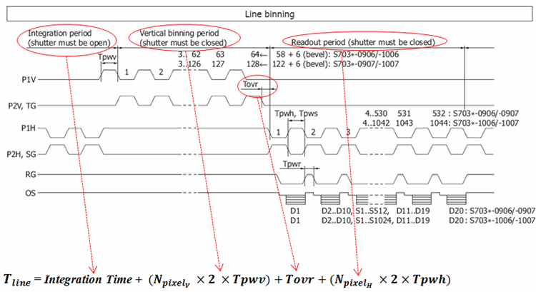
Figure 2. Line-binning timing diagram of FFT-CCD (S7030/S7031 series)
Based on this timing diagram, we can obtain the line time period Tline in which NpixelV is the CCD’s total vertical pixel count and NpixelH is the CCD’s total horizontal pixel count. Now, as an example, we calculate the min. line-binning and readout time of S7030/1-0906 using its min. timing values:
As a result, we obtain a max. possible line rate of 767Hz. Note that this rate assumes no integration time and is thus unrealistic; however, it provides a useful limit to guide further technical considerations.
Frame-readout mode
Please see the timing diagram below (also that of S7030/S7031 series of back-illuminated CCDs) for area-readout mode.
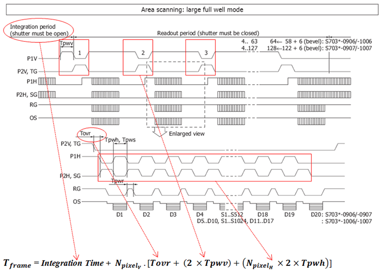
Figure 3. Area-scan timing diagram of S7030/S7031 series
Based on this timing diagram, we can obtain the CCD’s frame time (Tframe) by:
Equation 2.3b
For a numerical illustration, we calculate the min. frame readout time of S7030/1-0906 using its min. timing values:
And we obtain a max. possible frame rate of 1/35m ~ 28.5Hz as a result. Note that this rate assumes no integration time and is thus unrealistic; however, it provides a useful limit to guide further technical considerations.
It is noteworthy that S9970/S9971 and S9972/3 series of front-illuminated FFT-CCDs have similar timing diagrams and values, and thus, line/frame times and rates.
m x n binning frame-readout mode
Pixel binning in a 2D format (m × n format – n is the count of binned pixels in the vertical direction) is a common technique to diminish the effect of readout noise on SNR in low-light applications or to increase frame readout rate in high-speed applications; however, it comes with the tradeoff of deterioration in spatial resolution. In this readout arrangement, image frame time is:
Equation 2.3c
In 2D binning operation, note the summing gate (SG) input signal’s waveform would differ from that of the horizontal clock P2H; the period of SG would be m (count of horizontally binned pixels) times that of P2H with a “High” period that is (2m-1)/2m times that of Tpwh.
2.3.2 3-Phase CCD
The main family of Hamamatsu CCD products in this category is S10200/2-02/04/08/16-01 series of back-illuminated CCDs specialized for TDI operation. In 3-phase CCDs, there are no dopant barriers between pixel rows; instead, 2 of the clock phases act as electrical barriers during vertical charge transfers in order to avoid charge dispersion. As described in Hamamatsu’s TDI-CCD Technical Note, time-delay integration (TDI) is a CCD operation mode used in imaging of objects moving at a certain velocity in a known direction (example: screening of manufactured goods on a conveyor-belt inspection system).
TDI mode
Please see the timing diagram and parameters of HPK’s back-illuminated TDI-CCDs below:
Table 3. Timing parameter of a back-illuminated TDI-CCD
| Parameter | Symbol | Min. | Typ. | Max. | Unit | |
|---|---|---|---|---|---|---|
| P1V, 2V, 3V, TG | Pulse width | Tpwv | 120 | 770 | - | ns |
| Rise and fall times | Tprv,Tpfv | 2 | 10 | - | ns | |
| Overlap time | Tovrv | 30 | 300 | - | ns | |
| P1H, P2H | Pulse width | Tpwh | 12.5 | 16.5 | - | ns |
| Rise and fall times | Tprh, Tpfh | 3 | 6 | - | ns | |
| Duty ratio | - | - | 50 | - | % | |
| SG | Pulse width | Tpws | 12.5 | 16.5 | - | ns |
| Rise and fall times | Tprs, Tpfs | 2 | 4 | - | ns | |
| Duty ratio | - | - | 50 | - | % | |
| RG | Pulse width | Tpwr | 5 | 6 | - | ns |
| Rise and fall times | Tprr, Tpfr | 1 | 2 | - | ns | |
| TG-P1H | Overlap time | Tovr | 30 | 1000 | - | ns |
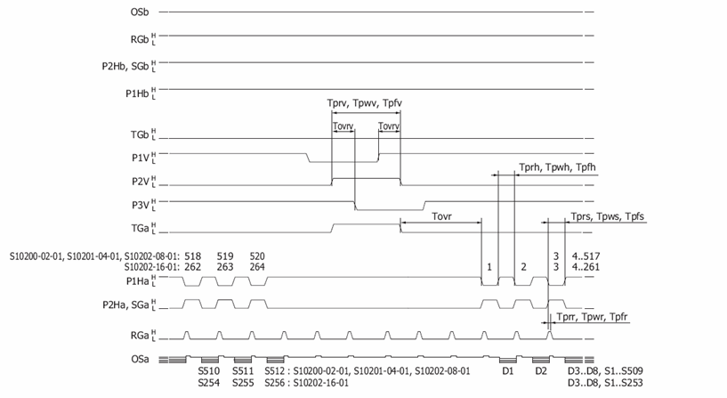
Figure 4. Timing diagram of a back-illuminated TDI-CCD
Based on the previous charts, we have:
Equation 2.3d
in which NpixelH is the number of pixels in the horizontal direction per output port. As an example, we calculate the min. TDI line readout time of S10202-16-01 using its min. timing values:
Consequently, its max. line rate in TDI mode is ~152KHz. Now, how about the typical timing values? Calculating this CCD’s line rate based on its typical timing values, we have: 300n + 770n + 1000n + (256 × 2 × 16.5) = 10.52μs, which yields a typical TDI line rate of 95KHz. This is a good example of what was emphasized earlier: that our calculations are purely theoretical and that sensor manufacturers and camera designers are likely to adopt more conservative or practical timing value based on experimental studies of signal integrity and waveform deterioration and actual noise measurements. It is noteworthy that Hamamatsu has specified a typical TDI line rate of 100KHz for S10202-16-01.
Line-binning mode
It would be a good exercise to see how line rate of S1020X series differs between TDI and line-binning operation modes. Towards that, using the above timing diagram, we develop the following formula for its line-binning operation:
Equation 2.3e
Using S10202-16-01’s min. timing values, we obtain its min. line-binning and readout time as:
And, consequently, max. possible line rate in line binning mode is ~33.9KHz. Note that this rate assumes no integration time and is hence unrealistic.
2.3.3 Resistive-gate CCD
As described in Hamamatsu’s corresponding technical note, this CCD’s architecture is one of a 1D array that operates in the global electronic shutter mode. The timing diagram and values of Hamamatsu’s sole series of RG-CCDs, S11155/6, in MPP operation mode are shown below. Before we discuss their timing characteristics, please note that MPP stands for multi-pinned phase; it is a technique by which electric potentials of CCD gates are inverted (i.e., made negative with respect to the silicon bulk) to attract holes to the Si/SiO2 interface for recombination with thermally generated or trapped electrons beneath the gates in order to suppress dark current and eliminate residual charge and image lag.
Table 4. Timing parameters of a resistive-gate CCD
| Parameter | Symbol | Min. | Typ. |
Max. |
Unit |
||
|---|---|---|---|---|---|---|---|
| ARG | Pulse width | Tpwar | - | - | - | µs | |
| Rise and fall times | Tprar, Tpfar | 200 | - | - | ns | ||
| REGH, REGL | Pulse width | Tpwreg | - | Tinteg-Tregtr | - | µs | |
| Rise and fall times | Tprreg, Tpfreg | 100 | - | - | ns | ||
| Transfer Time | S11155-2048-02 | Tregtr | 2 | 5 | - | µs | |
| S11156-2048-02 | 2 | 20 | - | ||||
| TG | Pulse width | Tpwv | 2 | - | - | µs | |
| Rise and fall times | Tprv, Tpfv | 20 | - | - | ns | ||
| P1H, P2H | Pulse width | Tpwh | 50 | 100 | - | ns | |
| Rise and fall times | Tprh, Tpfh | 10 | - | - | ns | ||
| Duty ratio | - | 40 | 50 | 60 | % | ||
| SG | Pulse width | Tpws | 50 | 100 | - | ns | |
| Rise and fall times | Tprs, Tpfs | 10 | - | - | ns | ||
| Duty ratio | - | 40 | 50 | 60 | % | ||
| RG | Pulse width | Tpwr | 5 | 15 | - | ns | |
| Rise and fall times | Tprr, Tpfr | 5 | - | - | ns | ||
| TG-P1H | Overlap time | Tovr | 1 | 2 | - | µs | |
| Integration time | S11155-2048-02 | Tinteg | 2 | 5 | - | µs | |
| S11156-2048-02 | 2 | 20 | - | µs | |||
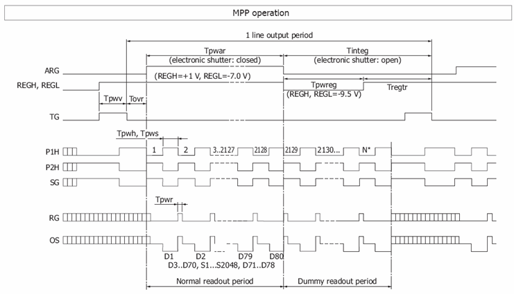
Figure 5. Timing diagram of a resistive-gate CCD
Based on the previous timing diagram, we obtain the CCD’s line time period (Tline) as:
Now, calculating min. line readout time of S11155/6-2048 in MPP mode using its min. timing values, we have:
And, we obtain a max. possible line rate of 1/215.8μs ~ 4.63KHz as a result. Note that this rate assumes no integration time and is thus unrealistic; however, it provides a useful limit to guide further technical considerations.
2.4 InGaAs image sensors
InGaAs is a compound semiconductor of group III elements, suitable for detection of light in the near-infrared wavelength region.
Since fabrication of transistors and other electronic circuitry on InGaAs is not feasible, silicon CMOS chips with the necessary signal processing functions (including charge amplifier) are wire-bonded (for front illumination) or bump-bonded (for back illumination) to an InGaAs photodiode array and used to bias, address, and read out the array’s pixels in various InGaAs image sensor products.
2.4.1 InGaAs linear array
We begin by studying the timing characteristics of G9211 to G9214 series and G9205 to G9208 series, which are products specialized for spectrometry.
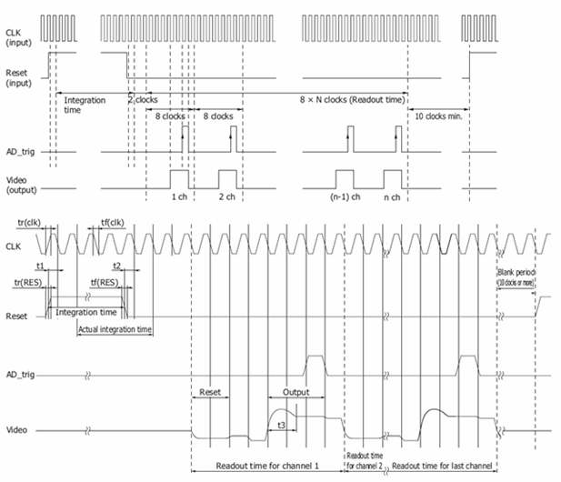
Figure 6. Timing diagram of an InGaAs linear array
Table 5. Timing parameters of an InGaAs linear array
| Parameter | Symbol | Min. | Typ. | Max. | Unit |
|---|---|---|---|---|---|
| Clock pulse frequency | - | 0.1 | - | 4 | MHz |
| Clock pulse width | tpw(clk) | 100 | - | - | ns |
| Clock pulse rise/fall times | tr(clk), tf(clk) | 0 | 20 | 100 | ns |
| Reset pulse width | tpw(RES) | 6000 | - | - | ns |
| Reset pulse rise/fall times | tr(RES), tf(RES) | 0 | 20 | 100 | ns |
| Reset (rise) timing | t1 | 50 | - | - | ns |
| Reset (fall) timing | t2 | 50 | - | - | ns |
| Output setting time | t3 | - | - | 600 | ns |
Based on the previous timing diagram, we obtain the InGaAs arrays’ line time period (Tline) as:
It is noteworthy that the array’s integration time is equal to (and set by) tpw(RES) but delayed by 3.tpw(CLK). Now, calculating min. Tline of a 512-pixel version of the array using its min. timing values, we have:
And, we obtain a max. line rate of 1/827.6μs ~ 1.2KHz as a result. Note that this rate has assumed the min. integration time of 6μs, which is the specified min. value of tpw(RES).
2.4.2 InGaAs focal-plane array (FPA)
At the time of this writing, Hamamatsu’s sole InGaAs FPA was G11097-0606S whose timing diagram and values are shown below.
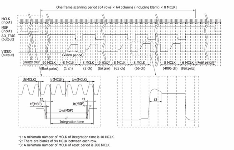
Figure 7. Timing diagram of G11097-0606S InGaAs FPA
Table 6. Timing parameters of G11097-0606S InGaAs FPA
| Parameter | Symbol | Min. | Typ. | Max. | Unit |
|---|---|---|---|---|---|
| Clock pulse rise/fall times | tr(MCLK) | 0 | 10 | 12 | ns |
| tf(MCLK) | |||||
| Clock pulse width | tpw(MCLK) | 10 | - | - | ns |
| Start pulse rise/fall times | tr(MSP) | 0 | 10 | 12 | ns |
| tf(MSP) | |||||
| Start pulse width*3 | tpw(MSP) | 0.001 | - | 10 | ms |
| Start (rise) timing*4 | t1 | 10 | - | - | ns |
| Start (fall) timing*4 | t2 | 10 | - | - | ns |
| Output setting time | t3 | - | - | 50 | ns |
*3: Integration time max.= 10 ms
*4: If the sensor is driven with these timings set shorter than the Min. value, then the operation may delay by 1 MCLK pulse.
Based on the timing diagram, we obtain G11097-0606S’s frame time (Tframe) as:
Now, calculating the FPA’s min. Tframe based on tpw(MCLK)’s min. value and a min. integration time of 40 × 2 × tpw(MCLK), we have:
And, we obtain a max. frame rate of 1/780.4μs ~ 1.28KHz as a result.
2.5 SNR calculations
In this section, we will conduct and review a number of case studies of image sensor SNR calculations. As part of this review, we will learn a number of key techniques to perform such calculations. As described earlier, please keep in mind that optical power [W] or electric current [A], whose dimensions are normalized to time, can be converted to units of photons or electrons per second (and vice versa) using Eq. 1.1a or the fundamental charge conversion constant (1.6E-19C/e-).
So, let’s study the following application conditions for applicable types of image sensors to see how measurement performances compare, but we will change the conditions as we proceed in order to discuss a number of key issues. Although these conditions are rather simplistic, they will effectively showcase how SNR calculations would be done in more complex scenarios.
i. Wavelength of 600nm, Incident photon flux of ~350K per sq. mm, Signal occurs every 1s
ii. Wavelength of 1500nm, Incident photon flux of ~350K per sq. mm, Signal occurs every 10ms
Note that the application conditions are fairly generic; many seemingly important details, such as what source is producing the light signal, do not affect these back-of-the-envelope calculations. Bear in mind that for an actual application, one must also find out how many data channels or pixels the customer would need and what pixel size would accommodate the desirable imaging resolution or spectral dispersion that the user has in mind. Commonly, this information can help to narrow down the range of selectable products. For the sake of our calculations, we assume that a channel count of 512 and a pixel size of ~24μm would suit the user’s purpose well in this spectrometric application.
We begin by using specs of S7030-0906 (back-illuminated CCD with 512 × 58 active pixels of 24μm in size) to calculate its max. dark output during a measurement: 1000e-/pixel/s × 1s = 1000e-/pixel. Using the application’s incident photon flux, we also calculate a light signal level of ~200 photons per pixel. With QE(600nm) = 92% and readout noise of 16e-, we calculate SNR using Eq. 1.3b to be:
Afterwards, we turn our attention to S9970-0906 (front-illuminated CCD with 512 × 60 active pixels of 24μm in size) and repeat the same calculations. We obtain a max. dark output of 3000e-/pixel/s × 1s = 3000e-/pixel. And so, with QE(600nm) = 34% and max. readout noise of 18e-, we calculate SNR using Eq. 1.3b to be:
It is noteworthy to mention that ‘excellent’ SNR is generally considered to be ≥10. Many users typically have a target performance of SNR > X in mind for which X is greater than 1 (even if less than 10). Thus, it is important to compare the results of such calculations with the value of X that represents the customer’s target SNR.
We populate Eq. 1.8 with the relevant values obtained above (and S7030-0906’s min. frame readout time of 35ms obtained in Section 2.3.1) and solve for Tintegration:
which yields an integration time of 1.25s. Note that both dark and photon signals are normalized to time (i.e., units of e-/s and photon/s have been utilized) in this calculation.
We assess that by using the vertical pixel counts in Eq. 1.3b to obtain:
Note that photoelectron charge was multiplied by the number of effective vertical pixels (in both numerator and denominator) while dark charge was multiplied by the total number of vertical pixels (in the denominator) in these calculations.
Suppose that the incident light in this case had a wavelength of 300nm. With S7030/S7031-0906’s QE(300nm) = 47%, we calculate SNR using Eq. 1.3b to be:
For comparison, we note that S9970-0906’s QE(300nm) = 7% (if phosphor-coated), and so we calculate SNR using Eq. 1.3b to be:
We repeat the calculations with the max. dark current of S9971-0906 (same CCD as S9970-0906 but with a thermoelectric cooler) at 0℃ to obtain a dark output charge of 150e-/pixel/s × 1s = 150e-/pixel and consequently obtain SNR as:
S7030-0906’s higher SNR in these calculations shows why back-illuminated CCDs are the premium image sensor solution for UV applications. Also, note the effect of cooling on dark shot noise and SNR.
Going back to our 600nm signal, we consider S3903-512Q (current-output NMOS linear image sensor with 512 pixels of 25μm in size). We begin by converting its max. dark current of 0.08pA to 5E5e-/pixel/s and thus obtain a charge output of 5E5e-/pixel in 1s.
Also, we convert its photosensitivity of 0.22A/W at 600nm to QE by the following relationship: QE = 124000 × Φ / λ in which Φ is photosensitivity [A/W], QE is a percentage, and λ is wavelength [nm]. We thus obtain QE = 45% at 600nm for S3903-512Q. Using the application’s incident photon flux, we also calculate a light signal level of 4340 photons per pixel. Now, note that the datasheet of S3903 does not specify a readout noise figure, but we assume a readout noise level of 1Ke- for a typical charge amplifier in this calculation. Thus, we obtain SNR as:
and hence conclude that S3903-512Q is barely suitable in this case due to its large dark shot noise and readout noise.
Suppose that instead of 4340 photons, 2 million photons were incident per pixel. Such a signal would produce more photoelectrons than the full-well capacities of horizontal registers of S7030 (1000Ke-) and S9970 (600Ke-) as applicable to line-binning mode. However, saturation charge of S3903 is the product of its photodiode capacitance and video-line bias voltage or 2pF × 2V = 4pC or 2.5E7 electrons. Calculating SNR of S3903 in such a scenario, we have:
We begin by studying specs of a standard InGaAs array like G9212-512S; extended InGaAs whose spectral response reaches over 2μm would be unnecessary in this case. Also, note that extended InGaAs has much higher levels of dark current and shot noise.
Using specs of G9212-512S, we convert its max. dark current of 5pA to 3.1E7 e-/pixel/s, resulting in a dark charge of 3.1E5 in 10ms. Alternatively, note that its max. dark output is also specified as 0.5V/s, which is equal to 5pA using the stated conversion efficiency of 16nV/e-. Furthermore, we convert its photosensitivity of 0.96A/W at 1500nm to QE = 79% at 1500nm. Using the application’s incident photon flux, we also calculate a light signal level of 2170 photons per pixel. We also obtain a max. readout noise of 18750e- using the specified value of 300μV rms and the stated conversion factor of 16nV/e-. With these figures, we calculate the SNR using Eq. 1.3b to be:
We populate Eq. 1.3b with the relevant values obtained above and solve for Nphoton:
Section 3. Measurement
Sometimes referred to by other names such as data point, a sampling, or an event, a measurement is a single experimental attempt [temporally (per a duration of time) and spatially (per a detector channel and within its physical size)] to quantify a signal. The result of a measurement is, thus, a piece of quantitative data that represents essential information about the true signal. Measurement is a very fundamental and seemingly simple concept, so why is it explored here? There are 3 important points to keep in mind.
3.1 Measurement frequency
Understanding the required sampling frequency for a measurement is of paramount importance to properly identify and define an application’s requirements and in order to compare those requirements with characteristics of candidate products.
Fundamentally, based on Nyquist’s sampling theorem, the measurement frequency is half of the sampling rate used to measure the signal. The following are examples of cases in which there is a detrimental mismatch between signal characteristics and measurement bandwidth:
- Using an imager with a spatial resolution of 10lp/mm to contact-image a min. feature size of 20μm. [Reason: 10lp/mm ~ 1mm /(2 × 10) = 50μm > 20μm]
- Using an oscilloscope with a sampling rate of 150MHz to look for multiple randomly occurring events with duration of 10ns each. (Reason: 150M < 2 × 1/10n = 200M)
3.2 Measurement range and resolution
Besides measurement frequency, the resolution of the measurement instrumentation in its ability to accurately resolve the smallest expected quantity of the measured parameter over the full range of its expected values is also of great importance.
The following are examples of cases in which there is a detrimental mismatch between signal characteristics and measurement resolution and range:
- Using an 8-bit ADC with a conversion factor of 1mV/LSB to digitize the output of an InGaAs LIS (G9494 series) with a saturation charge of 1.25E6 electrons and conversion factor of 1.6μV/e- (Reason: 1.25E6 × 1.6μ / 1m = 2000 > 2^8)
- Designing an amplifier circuit with BW = 1MHz to read out an image sensor with a max. pixel readout frequency of 2MHz.
- Using an InGaAs FPA (G11097-0606S) with a min. frame time of 780μs to separately image two bright NIR events (PW = 100ns) that occur 389μs apart.
- Using a spectrometer with a resolution of 30nm to distinguish emission or excitation peaks 10nm apart.
- Using a 16-bit/sample ADC with a bit rate of 5Mbps to digitize the output waveform of a CMOS image sensor with pixel readout rate of 400KHz (Reason: 5M / 16 < 400K)
3.3 Normalizations
While some signal characteristics (like amplitude, timing or frequency) can be appropriately obtained from measuring a single parameter (whether once or a multitude of times), others (like flux or power) would by definition include normalizations to time and/or spatial information and hence require measurements of 2 or more parameters in order to be quantified.
These differences are important, since a typical instrument designer is naturally concerned with the performance of her overall instrumentation: she could be designing an application condition that combines a series of measurements and contains one or more normalizations instead of consisting of a single parameter alone. In order to assess a photodetector’s suitability for a given application, one must bear that in mind and see how the way detector characteristics have been specified compares with the designer’s stated application conditions.
Towards that, one would begin by finding out to what temporal or spatial parameters a stated application condition might have been normalized; when in doubt, one should make sure about the dimension or unit of the application condition in question. However, it is also important to understand the scope of those normalizations. For example, one needs to examine whether the incident light “power” is applied to the entirety of a detector’s active area or if it’s normalized to pixel count or unit of area. As another example, it’s important to verify whether peak power or average power is meant when a customer refers to incident light “power”; peak and average power have different temporal normalizations in that the former is the ratio of energy content of a single pulse to the time duration of that pulse while the latter takes the time in between consecutive pulses into account. As a further example, if various spectral band components of a broad spectrum of light are to be detected by different detector channels separately (applicable to 1D or 2D serial- or parallel-readout multichannel detectors), performance of each detector channel must be assessed independently in accordance to its particular expected input light signal conditions.
Section 4. Conclusion
In conclusion, please bear in mind that multiple products could turn out to be suitable for a given set of application conditions. By taking price info into consideration, those options can be trimmed down to one or more candidates for evaluation.
- Confirmation
-
It looks like you're in the . If this is not your location, please select the correct region or country below.
You're headed to Hamamatsu Photonics website for US (English). If you want to view an other country's site, the optimized information will be provided by selecting options below.
In order to use this website comfortably, we use cookies. For cookie details please see our cookie policy.
- Cookie Policy
-
This website or its third-party tools use cookies, which are necessary to its functioning and required to achieve the purposes illustrated in this cookie policy. By closing the cookie warning banner, scrolling the page, clicking a link or continuing to browse otherwise, you agree to the use of cookies.
Hamamatsu uses cookies in order to enhance your experience on our website and ensure that our website functions.
You can visit this page at any time to learn more about cookies, get the most up to date information on how we use cookies and manage your cookie settings. We will not use cookies for any purpose other than the ones stated, but please note that we reserve the right to update our cookies.
1. What are cookies?
For modern websites to work according to visitor’s expectations, they need to collect certain basic information about visitors. To do this, a site will create small text files which are placed on visitor’s devices (computer or mobile) - these files are known as cookies when you access a website. Cookies are used in order to make websites function and work efficiently. Cookies are uniquely assigned to each visitor and can only be read by a web server in the domain that issued the cookie to the visitor. Cookies cannot be used to run programs or deliver viruses to a visitor’s device.
Cookies do various jobs which make the visitor’s experience of the internet much smoother and more interactive. For instance, cookies are used to remember the visitor’s preferences on sites they visit often, to remember language preference and to help navigate between pages more efficiently. Much, though not all, of the data collected is anonymous, though some of it is designed to detect browsing patterns and approximate geographical location to improve the visitor experience.
Certain type of cookies may require the data subject’s consent before storing them on the computer.
2. What are the different types of cookies?
This website uses two types of cookies:
- First party cookies. For our website, the first party cookies are controlled and maintained by Hamamatsu. No other parties have access to these cookies.
- Third party cookies. These cookies are implemented by organizations outside Hamamatsu. We do not have access to the data in these cookies, but we use these cookies to improve the overall website experience.
3. How do we use cookies?
This website uses cookies for following purposes:
- Certain cookies are necessary for our website to function. These are strictly necessary cookies and are required to enable website access, support navigation or provide relevant content. These cookies direct you to the correct region or country, and support security and ecommerce. Strictly necessary cookies also enforce your privacy preferences. Without these strictly necessary cookies, much of our website will not function.
- Analytics cookies are used to track website usage. This data enables us to improve our website usability, performance and website administration. In our analytics cookies, we do not store any personal identifying information.
- Functionality cookies. These are used to recognize you when you return to our website. This enables us to personalize our content for you, greet you by name and remember your preferences (for example, your choice of language or region).
- These cookies record your visit to our website, the pages you have visited and the links you have followed. We will use this information to make our website and the advertising displayed on it more relevant to your interests. We may also share this information with third parties for this purpose.
Cookies help us help you. Through the use of cookies, we learn what is important to our visitors and we develop and enhance website content and functionality to support your experience. Much of our website can be accessed if cookies are disabled, however certain website functions may not work. And, we believe your current and future visits will be enhanced if cookies are enabled.
4. Which cookies do we use?
There are two ways to manage cookie preferences.
- You can set your cookie preferences on your device or in your browser.
- You can set your cookie preferences at the website level.
If you don’t want to receive cookies, you can modify your browser so that it notifies you when cookies are sent to it or you can refuse cookies altogether. You can also delete cookies that have already been set.
If you wish to restrict or block web browser cookies which are set on your device then you can do this through your browser settings; the Help function within your browser should tell you how. Alternatively, you may wish to visit www.aboutcookies.org, which contains comprehensive information on how to do this on a wide variety of desktop browsers.
5. What are Internet tags and how do we use them with cookies?
Occasionally, we may use internet tags (also known as action tags, single-pixel GIFs, clear GIFs, invisible GIFs and 1-by-1 GIFs) at this site and may deploy these tags/cookies through a third-party advertising partner or a web analytical service partner which may be located and store the respective information (including your IP-address) in a foreign country. These tags/cookies are placed on both online advertisements that bring users to this site and on different pages of this site. We use this technology to measure the visitors' responses to our sites and the effectiveness of our advertising campaigns (including how many times a page is opened and which information is consulted) as well as to evaluate your use of this website. The third-party partner or the web analytical service partner may be able to collect data about visitors to our and other sites because of these internet tags/cookies, may compose reports regarding the website’s activity for us and may provide further services which are related to the use of the website and the internet. They may provide such information to other parties if there is a legal requirement that they do so, or if they hire the other parties to process information on their behalf.
If you would like more information about web tags and cookies associated with on-line advertising or to opt-out of third-party collection of this information, please visit the Network Advertising Initiative website http://www.networkadvertising.org.
6. Analytics and Advertisement Cookies
We use third-party cookies (such as Google Analytics) to track visitors on our website, to get reports about how visitors use the website and to inform, optimize and serve ads based on someone's past visits to our website.
You may opt-out of Google Analytics cookies by the websites provided by Google:
https://tools.google.com/dlpage/gaoptout?hl=en
As provided in this Privacy Policy (Article 5), you can learn more about opt-out cookies by the website provided by Network Advertising Initiative:
http://www.networkadvertising.org
We inform you that in such case you will not be able to wholly use all functions of our website.
Close

