Application notes


Technical notes
Ask an engineer


Publications
United States (EN)
Select your region or country.
InGaAs linear sensor reference circuit design - Section 3
John Gilmore, Lu Cheng, Hamamatsu Corporation
Scott Hunt, Analog Devices, Inc.
December 15, 2018
Section 1: Introduction
Section 2: System description
Section 3: Analog devices sensor board
Section 4: FPGA/USB processor data path
Section 5: FPGA/USB processor control/status path
Section 6: FPGA design description
Section 7: USB sub-system
Section 8: PC software and IGAA driver library
Section 9: Test results
This technical note is divided into nine sections. To navigate to any section, use the hyperlinks above.
Section 3: Analog Devices Sensor Board
3A. Theory of Operation and I2C and SPI Device Descriptions
Developed by Analog Devices, Inc. in collaboration with Hamamatsu, this board includes a Hamamatsu G920x InGaAs array, followed by two buffer amplifiers, a multiplexer to select a voltage from one of these two amplifiers, and a 1MSPS SAR ADC with integrated ADC driver. The board also includes a TEC controller and all of the required power conditioning to power the board from an AC adapter. The product selections were chosen to exceed the performance targets of the solution and provide high integration to enable a small footprint and simplicity of design. For more information about the devices chosen for use in this design, please refer to https://www.analog.com/en/technical-articles/integration-collab-at-heart-of-hi-perf-image-sensor-ref-design.html
Although the board does not conform to ANSI/VITA FMC standards due to the form factor and AC adapter power input, the connector area is designed to be able to interface with most FMC-compliant FPGA development boards in order to provide increased flexibility of target platform.
3B. Providing Power to the Board
Provide 9VDC, 1.5A or greater through barrel connector J2 (recommended: CUI, Inc. SMI24-9-V-P5 or similar). Although there is reverse power protection on the board, ensure that the polarity of the AC adapter is center positive for proper operation. For alternative InGaAs array variants, consider the power required by the TEC and ensure enough power is provided. This reference design board can support up to 3A maximum TEC current at up to 5V. A 9V, 2A AC adapter is enough to support a full 3A TEC current due to the high-efficiency 9V to 5V step-down buck regulator (the LTM8053) that is on the board. The power input features reverse protection, a 6A slow-blow fuse, and a 15V bidirectional TVS to protect the board from power supply transients. When using one of the G920x variants which has a 5V, 1.8A TEC, total power draw from the 9V AC wall adapter can be roughly 1.2A at maximum TEC drive.
3C. Array and Buffers
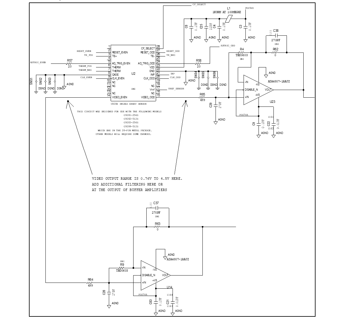
Figure 3-1: Sensor and buffers
Depending on the variant, the array has up to two analog outputs, called ‘Video-even’ and ‘Video-odd’, which are suggested to be buffered in the array datasheet. For the 512-pixel versions of the array, the even pixels come out on one line while the odd pixels are shifted out on the other line. The amplifier and filters are chosen to settle faster than the array, which specifies a 600ns output settling time. Provisions are included to match input resistances for the amplifier by placing 499Ω at R62 and R63 to reduce DC errors due to input bias current. If the 499Ω R62 and R63 are installed, it may be necessary to install C37 and C38 to neutralize the resulting input pole and avoid instability. The analog output of the array can go from 0.76V to 4.5V.
3D. Even-Odd Switch
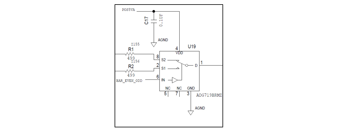
Figure 3-2: Even-odd multiplexer
A single-pole dual throw (SPDT) solid-state switch follows the even and odd pixel buffer amplifiers and connects one of the two to the ADC. A default pull-up resistor sets the switch to odd when floating, which is the correct side for the 256-pixel arrays. A 499Ω resistor ensures stability of the buffers driving the switch capacitance and reduces current spikes during switching.
3E. ADC Driver and ADC
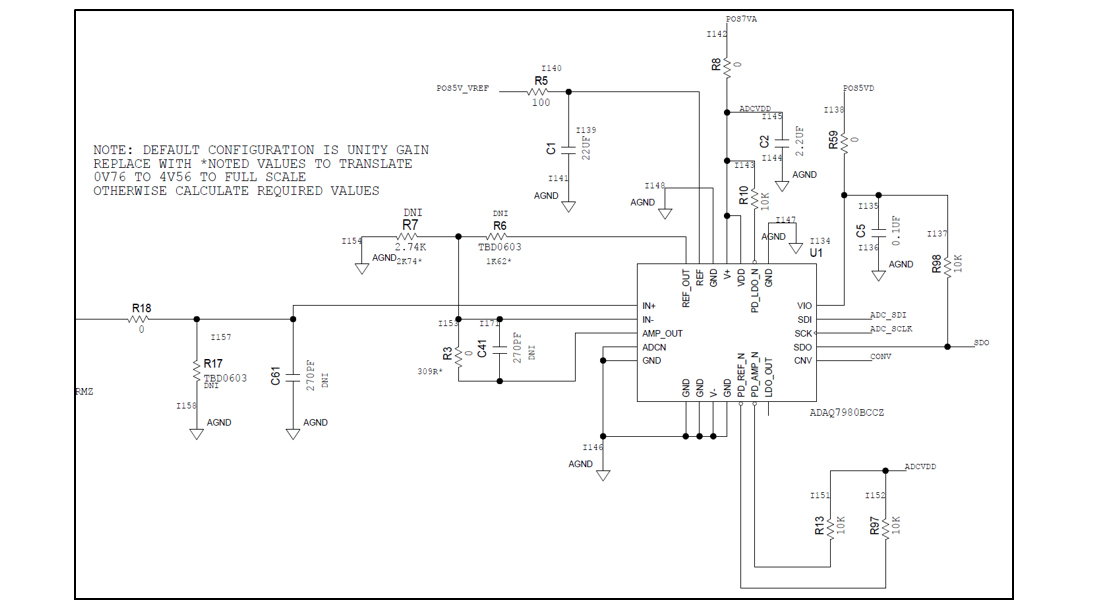
Figure 3-3: ADC
The ADC driver is integrated into the ADAQ7980. By default, this stage is in unity-gain, which provides the optimal settling and does not negatively affect the noise. Provisions and recommendations are included to match the input to the full-scale 0-5V input range of the ADC if desired. The ADAQ7980 ADC is a 16-bit, 1MSPS SAR ADC with an integrated ADC driver, reference buffer, LDO, and necessary passives that is connected to the SPI bus. For more information about this integrated signal chain, refer to https://www.analog.com/en/technical-articles/integration-collab-at-heart-of-hi-perf-image-sensor-ref-design.html. The reference voltage is 5V, so one LSB represents 76.3µV.
3F. Serial Devices
There are a total of 4 serial devices on the reference board:
SPI Bus
- One AD5235 dual 25kΩ, 1024-position digital potentiometer
- One ADAQ7980 16-bit ADC
I2C Bus
- One AD7991 12-bit ADC
- One AD5627 12-bit DAC
3G. AD5235 Dual Potentiometer and Bias Divider
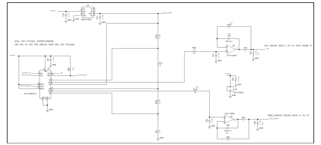
Figure 3-4: Dual POT for Vref and INP bias voltages
The programmable bias voltages for the sensor are derived from a voltage divider off of the precision ADR4550 5V voltage reference used for the ADC. Potentiometer 1 controls the INP voltage from approximately 2.5V at maximum code to approximately 5V at minimum code. Potentiometer 2 controls the VREF_SENSOR voltage from approximately 1V at minimum code to approximately 2V at maximum code. When potentiometer 1 is set to its lowest value of 0, the INP voltage is 5V. When INP is set to the maximum value of 1023, the INP voltage is 2.5V. Intermediate values can be calculated according to the following equation:
Equation 1
where D can range from 0 to 1023. Note that although the AD8606 is a ‘rail to rail’ output amplifier, it will only get to about 4.96V, so writing values lower than ‘16’ to the rheostat may not result in the desired output. This should not be a problem because the maximum bias voltage specified in the G920x datasheet is 4.6V. The default value written to this rheostat should be 205d (0xCD) to get 4.5V.
Potentiometer 2 controls the Vref voltage going to the array. When the potentiometer is set to its lowest value of 0, the output on the Vref pin is 1V. When the potentiometer is set to its highest value of 1024, the output on the Vref pin is 2V. Intermediate values can be calculated according to the following equation:
Equation 2
where D can range from 0 to 1023. Vref should be set to a default value of 1.26V by writing 266d to the potentiometer (0x10A).
3H. AD7991 ADC
Note: I2C address: 010 1001
The AD7991 is a 12-bit ADC with a 2.5V reference provided by the ADN8835, so each LSB represents 610μV. Channel 0 is used to measure the amplified and linearized thermistor output from the ADN8835.
The thermistor uses a simple linearization circuit that results in an output of approximately 26.53mV/°C from -10°C to 40°C, with an offset of 0.566V.
To convert from volts to approximate temperature, use the following equation:
Equation 3
This approximation will result in errors of slightly over 1°C at -10°C and 40°C, and nearly zero error at 15°C. Note that it is possible to write voltages lower than 0.239V, which will result in a lower setpoint temperature. However, the above approximation will result in large errors. For example, the equation above predicts that 0V corresponds to -21.3°C, while the true temperature would be close to -29°C.
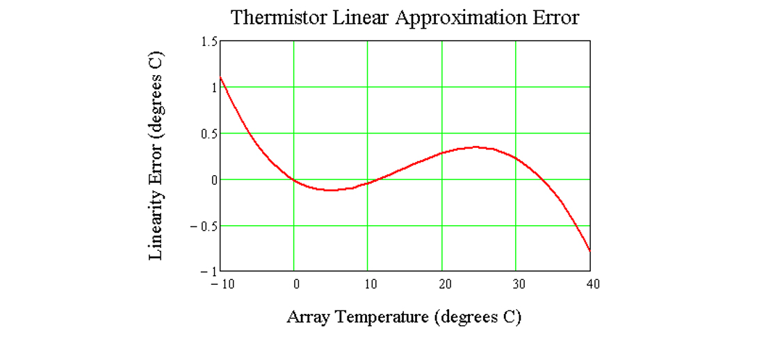
Figure 3-5: Thermistor linear approximation error
If higher accuracy conversion is required, use the following equation:
Equation 4
where:
Temperature = The thermistor temperature in degrees Kelvin
Tr = 298.15K (Temperature at which nominal thermistor resistance is specified)
Rr = 5kΩ (Nominal thermistor resistance at Tr)
B = 3200K (Thermistor constant given in the datasheet)
Rx = 5.11kΩ (R43 in the schematic)
Rtop = 10kΩ (R32 in the schematic)
Rfb = 12kΩ (R31 in the schematic)
Note: Using this equation results in linearity error dominated by the number format precision used, and should be negligible if implemented in floating point on a PC.
Channel 1 is used to measure the linearized thermistor output from the ‘hot’ side of the heatsink. The same equation as above can be used to convert volts to temperature, assuming the same thermistor is used. Note that once again, the approximate equation will lose accuracy above 40°C, and the full equation should be used if higher temperatures are expected. If a different thermistor is used, then the equation will vary depending on the thermistor’s characteristics. For proper operation, the REF_SEL bit in the AD7991’s Configuration Register must be set to ‘1’ (this uses the Vin3/Vref pin as the converter reference).
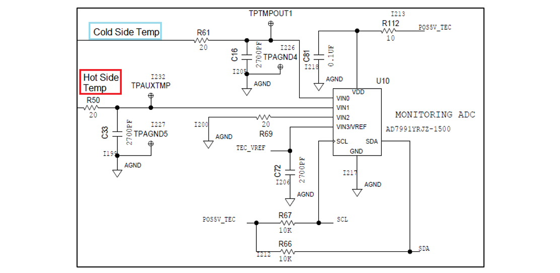
Figure 3-6: Temperature monitoring ADC
3I. DAC
Note: I2C address: 000 1110
The AD5627 DAC controls the temperature setpoint for the TEC controller. To calculate the temperature setpoint based on the output data written, use the following equation:
Equation 5
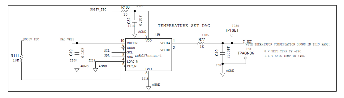
Figure 3-7: Temperature setting DAC
3J. TEC Controller
The ADN8835, a TEC controller with integrated 3A power FETs, is used to very accurately control the temperature of the image sensor array. The AD5627 sets the temperature setpoint and the AD7991 reads the hot side and cold side thermistor temperatures. The TEC Voltage Limit and Current Limit are set by resistor dividers tailored to the values needed for the G920x family. To change these limits to accommodate a different family of image sensors with different TEC requirements, see Analog Devices UG-951 for suggestions on the resistor value. For more information on thermoelectric cooler control, refer to ADN8835 datasheet. It may also be necessary to adjust the analog PID components and thermistor components in order to accommodate other sensors. The EN/SY pin is pulled up in order to be enabled by default, but the TEC controller can be shut down if this signal is pulled low by the FPGA. This pin can also be used for synchronization, as described below.
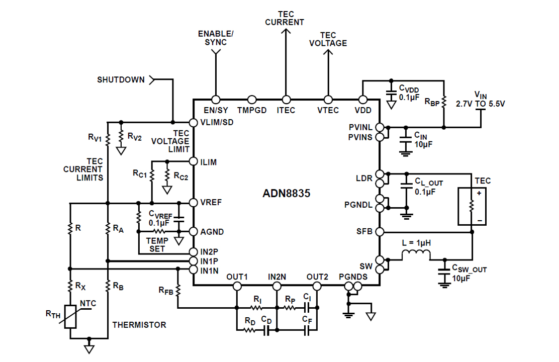
Figure 3-8: TEC control
Indicators and Test Points
Ultralow power LEDs are provided to indicate temp good from the ADN8835 (DS4) and power good for all power rails: DS3 indicates POS5V_TEC, DS2 indicates POS7VA, and DS1 indicates POS5VD/POS5VA power good. Surface mount test points are provided for many signals to be probed, especially in the dense TEC control portion of the circuit, along with corresponding ground test points.
Synchronization Feature and LTM8053 Modes
To remove any switching clock intermodulation from the circuit, this design can be fully synchronized. ADN8835 can be synchronized by driving the shutdown signal, BAR_TEC_SD, with a clock between 1.85MHz and 3.25MHz. LTM8053 can also be synchronized by installing a provisional zero ohm resistor in position R35 to connect its SYNC pin to the BAR_TEC_SD signal. This reduces the maximum synchronization clock frequency to 3MHz. The clocks of both of these devices may be synchronized to a clock output from the FPGA that is synchronous with the sensor pixel clock signals, and the ADAQ7980 samples may be taken at integer multiples of the sync clock frequency, eliminating the effect of switching noise on the measurement. For more information, see the notes on the schematic and the ADN8835 and LTM8053 datasheets. The full complement of SYNC/MODE options for LTM8053 are described in the schematic. By default, the ADN8835 and the LTM8053 are both running on their internal clocks and the LTM8053 is in pulse-skip mode.
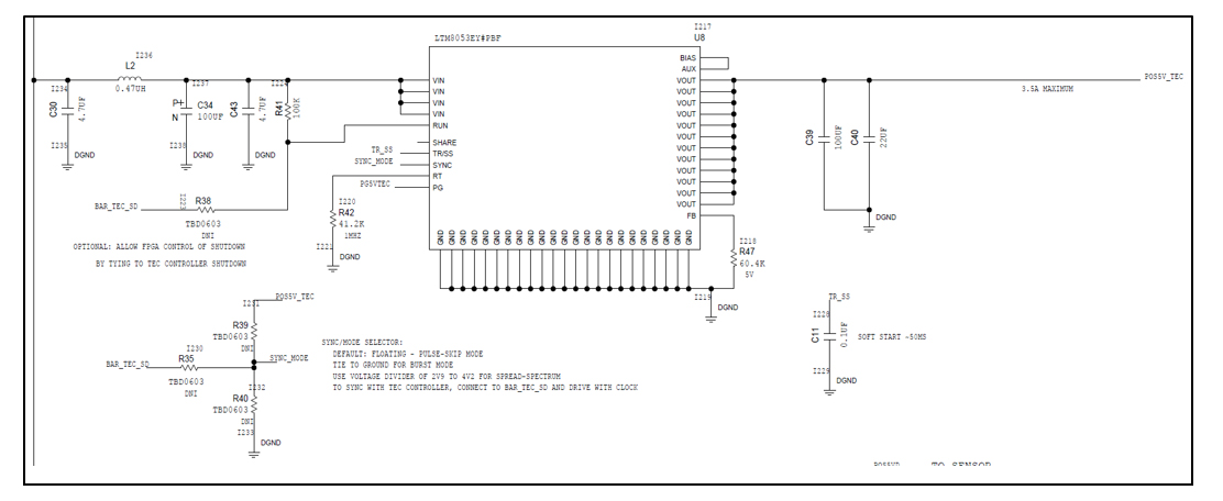
Figure 3-9: SYNC / mode selection
- Confirmation
-
It looks like you're in the . If this is not your location, please select the correct region or country below.
You're headed to Hamamatsu Photonics website for US (English). If you want to view an other country's site, the optimized information will be provided by selecting options below.
In order to use this website comfortably, we use cookies. For cookie details please see our cookie policy.
- Cookie Policy
-
This website or its third-party tools use cookies, which are necessary to its functioning and required to achieve the purposes illustrated in this cookie policy. By closing the cookie warning banner, scrolling the page, clicking a link or continuing to browse otherwise, you agree to the use of cookies.
Hamamatsu uses cookies in order to enhance your experience on our website and ensure that our website functions.
You can visit this page at any time to learn more about cookies, get the most up to date information on how we use cookies and manage your cookie settings. We will not use cookies for any purpose other than the ones stated, but please note that we reserve the right to update our cookies.
1. What are cookies?
For modern websites to work according to visitor’s expectations, they need to collect certain basic information about visitors. To do this, a site will create small text files which are placed on visitor’s devices (computer or mobile) - these files are known as cookies when you access a website. Cookies are used in order to make websites function and work efficiently. Cookies are uniquely assigned to each visitor and can only be read by a web server in the domain that issued the cookie to the visitor. Cookies cannot be used to run programs or deliver viruses to a visitor’s device.
Cookies do various jobs which make the visitor’s experience of the internet much smoother and more interactive. For instance, cookies are used to remember the visitor’s preferences on sites they visit often, to remember language preference and to help navigate between pages more efficiently. Much, though not all, of the data collected is anonymous, though some of it is designed to detect browsing patterns and approximate geographical location to improve the visitor experience.
Certain type of cookies may require the data subject’s consent before storing them on the computer.
2. What are the different types of cookies?
This website uses two types of cookies:
- First party cookies. For our website, the first party cookies are controlled and maintained by Hamamatsu. No other parties have access to these cookies.
- Third party cookies. These cookies are implemented by organizations outside Hamamatsu. We do not have access to the data in these cookies, but we use these cookies to improve the overall website experience.
3. How do we use cookies?
This website uses cookies for following purposes:
- Certain cookies are necessary for our website to function. These are strictly necessary cookies and are required to enable website access, support navigation or provide relevant content. These cookies direct you to the correct region or country, and support security and ecommerce. Strictly necessary cookies also enforce your privacy preferences. Without these strictly necessary cookies, much of our website will not function.
- Analytics cookies are used to track website usage. This data enables us to improve our website usability, performance and website administration. In our analytics cookies, we do not store any personal identifying information.
- Functionality cookies. These are used to recognize you when you return to our website. This enables us to personalize our content for you, greet you by name and remember your preferences (for example, your choice of language or region).
- These cookies record your visit to our website, the pages you have visited and the links you have followed. We will use this information to make our website and the advertising displayed on it more relevant to your interests. We may also share this information with third parties for this purpose.
Cookies help us help you. Through the use of cookies, we learn what is important to our visitors and we develop and enhance website content and functionality to support your experience. Much of our website can be accessed if cookies are disabled, however certain website functions may not work. And, we believe your current and future visits will be enhanced if cookies are enabled.
4. Which cookies do we use?
There are two ways to manage cookie preferences.
- You can set your cookie preferences on your device or in your browser.
- You can set your cookie preferences at the website level.
If you don’t want to receive cookies, you can modify your browser so that it notifies you when cookies are sent to it or you can refuse cookies altogether. You can also delete cookies that have already been set.
If you wish to restrict or block web browser cookies which are set on your device then you can do this through your browser settings; the Help function within your browser should tell you how. Alternatively, you may wish to visit www.aboutcookies.org, which contains comprehensive information on how to do this on a wide variety of desktop browsers.
5. What are Internet tags and how do we use them with cookies?
Occasionally, we may use internet tags (also known as action tags, single-pixel GIFs, clear GIFs, invisible GIFs and 1-by-1 GIFs) at this site and may deploy these tags/cookies through a third-party advertising partner or a web analytical service partner which may be located and store the respective information (including your IP-address) in a foreign country. These tags/cookies are placed on both online advertisements that bring users to this site and on different pages of this site. We use this technology to measure the visitors' responses to our sites and the effectiveness of our advertising campaigns (including how many times a page is opened and which information is consulted) as well as to evaluate your use of this website. The third-party partner or the web analytical service partner may be able to collect data about visitors to our and other sites because of these internet tags/cookies, may compose reports regarding the website’s activity for us and may provide further services which are related to the use of the website and the internet. They may provide such information to other parties if there is a legal requirement that they do so, or if they hire the other parties to process information on their behalf.
If you would like more information about web tags and cookies associated with on-line advertising or to opt-out of third-party collection of this information, please visit the Network Advertising Initiative website http://www.networkadvertising.org.
6. Analytics and Advertisement Cookies
We use third-party cookies (such as Google Analytics) to track visitors on our website, to get reports about how visitors use the website and to inform, optimize and serve ads based on someone's past visits to our website.
You may opt-out of Google Analytics cookies by the websites provided by Google:
https://tools.google.com/dlpage/gaoptout?hl=en
As provided in this Privacy Policy (Article 5), you can learn more about opt-out cookies by the website provided by Network Advertising Initiative:
http://www.networkadvertising.org
We inform you that in such case you will not be able to wholly use all functions of our website.
Close