Application notes

Technical notes
Ask an engineer


Publications
United States (EN)
Select your region or country.
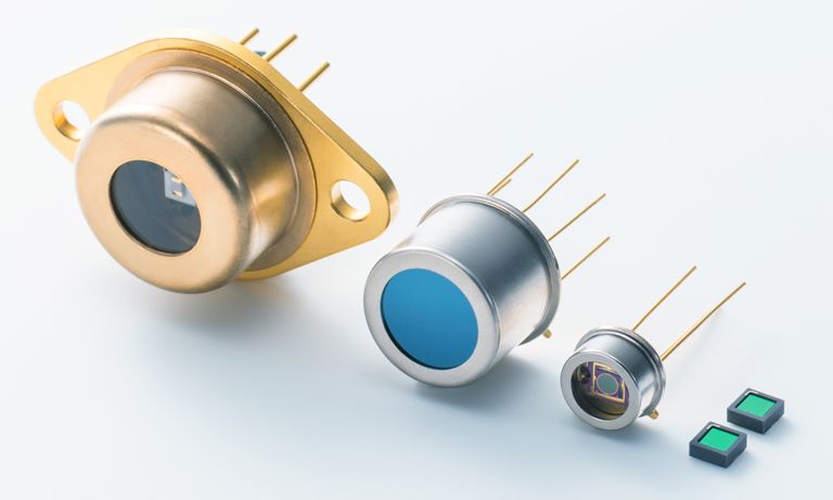
A technical guide to silicon photomultipliers (MPPC) - Overview
Ardavan Ghassemi, Hamamatsu Corporation
Kota Kobayashi & Kenichi Sato, Hamamatsu Photonics K.K.
January 11, 2018
Silicon photomultipliers from Hamamatsu are called Multi-Pixel Photon Counters (MPPC). This extensive guide to MPPCs describes the device's operating principle, its performance parameters, and how to measure various characteristics such as gain, breakdown voltage, photon detection efficiency, and linearity. Also included is a detector selection case study where, for a given set of measurement conditions, the signal-to-noise ratio and linearity of an avalanche photodiode and an MPPC are calculated and compared.
Table of Contents:
Section 1: Operation principles and characteristics
1-1. The PN junction & unity-gain Si photodiodes
1-2. Avalanche photodiodes (APD)
1-3. MPPC (Multi-Pixel Photon Counter)
Section 2: APD & MPPC performance parameters
2-1. Signal
2-2. Noise
2-3. Signal-to-noise ratio (S/N)
2-4. Linearity
2-5. Dynamic range
2-6. Time response
2-7. Time resolution
Section 3: Case studies of APD/MPPC performance calculations
3-1. Calculating an MPPC's signal-to-noise ratio
3-2. Calculating an MPPC's linearity
3-3. Calculating an APD's signal-to-noise ratio
3-4. Calculating an APD's linearity
3-5. Conclusion
Section 4: MPPC characterization measurements
4-1. Gain and breakdown voltage
4-2. Breakdown voltage measurement by obtaining Vpeak from I-V curve
4-3. Photon detection efficiency (PDE) vs. bias voltage measurement
4-4. Dark count rate (DCR) and prompt crosstalk measurement using counter and CR filter
4-5. Measurement of DCR, prompt crosstalk, recovery time, afterpulsing, and delayed crosstalk using digitizer and digital pulse processing
4-6. Single-photon pulse shape measurement
4-7. Time resolution: coincidence time resolution (CTR) and single photon time resolution (SPTR)
4-8. Dynamic range and linearity
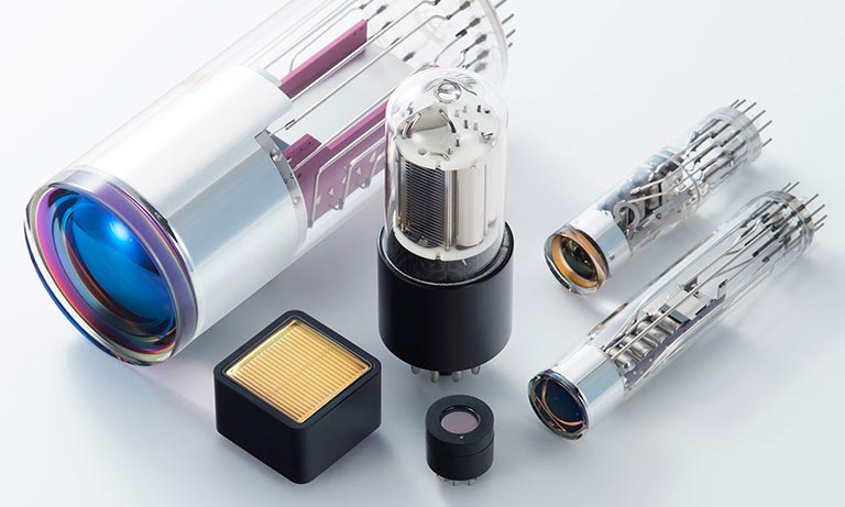
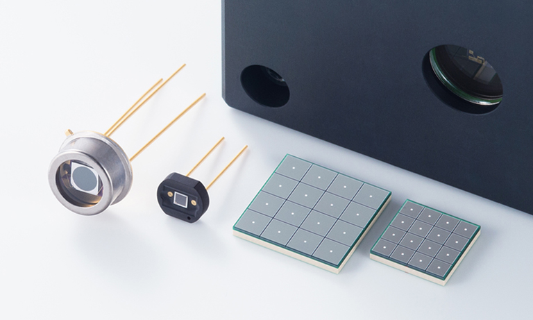
Overview: Silicon as a photodetector technology
Over recent years, various optical applications have experienced a shift in their optimal choice of photodetector technology. This shift has followed a general trend away from the vacuum-based photomultiplier tube (PMT) towards solid-state silicon photodetectors. In addition to the greater cost efficiency of silicon device microfabrication and scalability of wafer processing, several technological advantages based on physical properties of silicon photodetectors have contributed to that trend:
- Considering silicon’s narrow bandgap (1.14 eV) and due to higher transition probability of a photoelectron from a silicon crystal’s valence band to its conduction band than emission probability of a photoelectron from an alkali-based photocathode to the vacuum level, silicon photodetectors can attain higher quantum efficiencies over a wider range of wavelengths (UV-VIS-NIR) than the PMT.
- Silicon’s semiconductor properties and crystalline structure allow for formation of extrinsically-doped regions that can be depleted of charge carriers (electrons or holes) in presence of an electric field, hence diminishing carrier recombination. This, along with high (excess) carrier drift velocity in the depleted regions, provides for a higher collection efficiency of photoelectron charge (i.e. less photoelectric signal loss) than the likelihood of a photoelectron creating secondary electron emissions in bombarding a PMT’s first dynode.
- Fine feature sizes attainable by modern silicon microfabrication processing allow the implementation of micron-sized PN junctions and anode/cathode regions. Combined with high electrical conductance of doped silicon, that permits the formation of strong electric field (E-field) intensities within a silicon detector’s depletion layer. This enables low-voltage operation of silicon photodetectors at low supply currents, resulting in low power consumption. Furthermore, at sufficiently strong E-field intensities, a high carrier multiplication or avalanche gain within small physical dimensions of a silicon device is made possible; this internal gain mechanism is fundamental to increasing the signal level to above the noise floor of an output amplifier for signal readout. Additionally, small PN junction and anode/cathode physical dimensions result in small junction capacitance, which facilitates high-frequency response.
- When a photosensitive area larger than what monolithic chips (as restricted by wafer size) can accommodate is required, compactness of silicon photodetectors with a high fill-factor (i.e. ratio of photosensitive area to total area) permits the construction of large focal-plane arrays of tiled chips with ultrahigh (≤200 μm of dead gap) packing-efficiency.
- Silicon photodetectors are mechanically rugged and are not hampered by effects of magnetic field, hysteresis, and aging/warmup considerations unlike PMTs.
- Despite the above strengths of silicon photodetectors, it should be noted that the PMT has lower dark current output per unit of photosensitive area, less capacitance per unit of area, and greater radiation hardness.
- It is also noteworthy to add that silicon is the material of choice for VLSI microelectronic fabrication of mixed-signal (analog + digital) ICs, based specifically on CMOS transistors that are essential to implementation of modern signal processing schemes. Furthermore, silicon’s native oxide has excellent light transmittance while silicon itself is opaque; this enables microfabrication of mirrors, waveguides, and gratings on silicon wafers. Additionally, since silicon has remarkable mechanical strength and rigidity, various three-dimensional dynamic (actuators, oscillators, etc.) or static (capacitors, inductors, bonding and anchoring pads, and other fixtures) structures can be constructed on silicon wafers via wet or dry etching processes based on particular lattice orientations. These fabrication technologies lead to integration of silicon photodetectors into MOEMS (micro-opto-electro-mechanical systems) products with tremendous potential in a wide variety of optical applications that demand large-scale cost-effective manufacturing, dimensional miniaturization, and ultralow power consumption; a similar integration of PMT is not possible due to its inherent dimensional and power-consumption limitations. Altogether, a technological revolution, known as Lab-on-Chip (LoC), of micron-scale wafer-level integration of optical measurement, photoelectric signal processing, and digital data output with enormous potential in biomedical, scientific/analytical, industrial, and consumer markets is underway as a result.
- Confirmation
-
It looks like you're in the . If this is not your location, please select the correct region or country below.
You're headed to Hamamatsu Photonics website for US (English). If you want to view an other country's site, the optimized information will be provided by selecting options below.
In order to use this website comfortably, we use cookies. For cookie details please see our cookie policy.
- Cookie Policy
-
This website or its third-party tools use cookies, which are necessary to its functioning and required to achieve the purposes illustrated in this cookie policy. By closing the cookie warning banner, scrolling the page, clicking a link or continuing to browse otherwise, you agree to the use of cookies.
Hamamatsu uses cookies in order to enhance your experience on our website and ensure that our website functions.
You can visit this page at any time to learn more about cookies, get the most up to date information on how we use cookies and manage your cookie settings. We will not use cookies for any purpose other than the ones stated, but please note that we reserve the right to update our cookies.
1. What are cookies?
For modern websites to work according to visitor’s expectations, they need to collect certain basic information about visitors. To do this, a site will create small text files which are placed on visitor’s devices (computer or mobile) - these files are known as cookies when you access a website. Cookies are used in order to make websites function and work efficiently. Cookies are uniquely assigned to each visitor and can only be read by a web server in the domain that issued the cookie to the visitor. Cookies cannot be used to run programs or deliver viruses to a visitor’s device.
Cookies do various jobs which make the visitor’s experience of the internet much smoother and more interactive. For instance, cookies are used to remember the visitor’s preferences on sites they visit often, to remember language preference and to help navigate between pages more efficiently. Much, though not all, of the data collected is anonymous, though some of it is designed to detect browsing patterns and approximate geographical location to improve the visitor experience.
Certain type of cookies may require the data subject’s consent before storing them on the computer.
2. What are the different types of cookies?
This website uses two types of cookies:
- First party cookies. For our website, the first party cookies are controlled and maintained by Hamamatsu. No other parties have access to these cookies.
- Third party cookies. These cookies are implemented by organizations outside Hamamatsu. We do not have access to the data in these cookies, but we use these cookies to improve the overall website experience.
3. How do we use cookies?
This website uses cookies for following purposes:
- Certain cookies are necessary for our website to function. These are strictly necessary cookies and are required to enable website access, support navigation or provide relevant content. These cookies direct you to the correct region or country, and support security and ecommerce. Strictly necessary cookies also enforce your privacy preferences. Without these strictly necessary cookies, much of our website will not function.
- Analytics cookies are used to track website usage. This data enables us to improve our website usability, performance and website administration. In our analytics cookies, we do not store any personal identifying information.
- Functionality cookies. These are used to recognize you when you return to our website. This enables us to personalize our content for you, greet you by name and remember your preferences (for example, your choice of language or region).
- These cookies record your visit to our website, the pages you have visited and the links you have followed. We will use this information to make our website and the advertising displayed on it more relevant to your interests. We may also share this information with third parties for this purpose.
Cookies help us help you. Through the use of cookies, we learn what is important to our visitors and we develop and enhance website content and functionality to support your experience. Much of our website can be accessed if cookies are disabled, however certain website functions may not work. And, we believe your current and future visits will be enhanced if cookies are enabled.
4. Which cookies do we use?
There are two ways to manage cookie preferences.
- You can set your cookie preferences on your device or in your browser.
- You can set your cookie preferences at the website level.
If you don’t want to receive cookies, you can modify your browser so that it notifies you when cookies are sent to it or you can refuse cookies altogether. You can also delete cookies that have already been set.
If you wish to restrict or block web browser cookies which are set on your device then you can do this through your browser settings; the Help function within your browser should tell you how. Alternatively, you may wish to visit www.aboutcookies.org, which contains comprehensive information on how to do this on a wide variety of desktop browsers.
5. What are Internet tags and how do we use them with cookies?
Occasionally, we may use internet tags (also known as action tags, single-pixel GIFs, clear GIFs, invisible GIFs and 1-by-1 GIFs) at this site and may deploy these tags/cookies through a third-party advertising partner or a web analytical service partner which may be located and store the respective information (including your IP-address) in a foreign country. These tags/cookies are placed on both online advertisements that bring users to this site and on different pages of this site. We use this technology to measure the visitors' responses to our sites and the effectiveness of our advertising campaigns (including how many times a page is opened and which information is consulted) as well as to evaluate your use of this website. The third-party partner or the web analytical service partner may be able to collect data about visitors to our and other sites because of these internet tags/cookies, may compose reports regarding the website’s activity for us and may provide further services which are related to the use of the website and the internet. They may provide such information to other parties if there is a legal requirement that they do so, or if they hire the other parties to process information on their behalf.
If you would like more information about web tags and cookies associated with on-line advertising or to opt-out of third-party collection of this information, please visit the Network Advertising Initiative website http://www.networkadvertising.org.
6. Analytics and Advertisement Cookies
We use third-party cookies (such as Google Analytics) to track visitors on our website, to get reports about how visitors use the website and to inform, optimize and serve ads based on someone's past visits to our website.
You may opt-out of Google Analytics cookies by the websites provided by Google:
https://tools.google.com/dlpage/gaoptout?hl=en
As provided in this Privacy Policy (Article 5), you can learn more about opt-out cookies by the website provided by Network Advertising Initiative:
http://www.networkadvertising.org
We inform you that in such case you will not be able to wholly use all functions of our website.
Close