Application notes

Technical notes
Ask an engineer


Publications
United States (EN)
Select your region or country.
Physics and operation of the MPPC silicon photomultiplier
Slawomir Piatek, PhD, Hamamatsu Corporation & New Jersey Institute of Technology
February 2, 2014
Introduction
The Multi-Pixel Photon Counter (also known as a silicon photomultiplier or SiPM) is a solid-state device capable of detecting individual photons. The geometrical structure of an MPPC is a rectangular array of square pixels where each pixel is a series connection of an avalanche photodiode (APD) operating in Geiger mode and a quenching resistor (RQ). All of the pixels are identical and connected in parallel (see Figure 1). An external power source reverse-biases the array to a voltage VBIAS that is up to a few volts above the breakdown voltage (VBR) of an APD. The difference between VBIAS and VBR is commonly referred to as overvoltage (ΔV), which is one of the most important operational parameters of an MPPC. Depending on the design of a pixel, VBR is in the 30 to 70 V range.
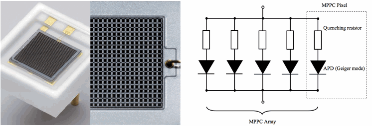
Figure 1. Close-up view of an MPPC sensor (left). Equivalent circuit of an MPPC array (right). Each pixel consists of a light-sensitive APD operating in Geiger mode connected in series with a quenching resistor. An external power source reverse-biases the array to a voltage that is up to a few volts above the breakdown voltage of an APD.
When a single photon strikes and penetrates a pixel, the photon can excite an electron into the conduction band and thus create a mobile electron-hole (e-h) pair. The internal electric field separates the pair and directs the electron (or hole) into the avalanche region where, through impact ionization, the charge carrier initiates a current avalanche. As the current builds up, the voltage on RQ increases, whereas the voltage on the APD decreases. The lower voltage on the APD reduces the probability of impact ionization; thus, the current avalanche reaches a maximum and then declines — it is being quenched. The resulting signal is a fast current pulse with a rise time of ~1 ns, a peak value proportional to ΔV/RQ, and a fall-off time on the order of tens of ns. In the fall-off phase, the voltage on the APD increases reaching the pre-avalanche value once the avalanche is completely quenched. An avalanche can produce 105 to 106 additional e-h pairs depending on ΔV. The number of the additional e-h pairs is the gain (M). If the same pixel absorbs two or more photons simultaneously, the resulting current pulse has the same amplitude and duration as that due to a single photon. However, if distinct pixels absorb photons simultaneously, the resulting pulse is a superposition of the single-photon pulses; its amplitude is proportional to the number of independently "fired" pixels.
Because of its high internal gain, an MPPC is an alternative to a photomultiplier tube (PMT). Additional characteristics such as immunity to magnetic fields, low-voltage operation, smaller size, and much longer lifetime all make MPPCs preferred alternatives to PMTs.
This article reviews the physics of an MPPC as well as its operational, optical, and electrical characteristics. Section I describes the physics of an APD—the building block of an MPPC. Section II discusses the operation of a pixel in an MPPC. Section III describes a typical structure of an MPPC. Sections IV and V discuss performance and opto-electrical characteristics, respectively. The article concludes with a summary of the key points.
Section I: The physics of an APD
Central to the operation of an APD as a photodetector is the presence of a p-n junction in its structure. The middle panel of Figure 2 shows schematically the typical p+- p - n construction of an APD. The structure is externally reverse-biased by VBIAS, which, together with the intrinsic electric field of the p-n junction, create an electric field whose strength profile is schematically shown in the top panel. The field is maximum at the metallurgical junction.
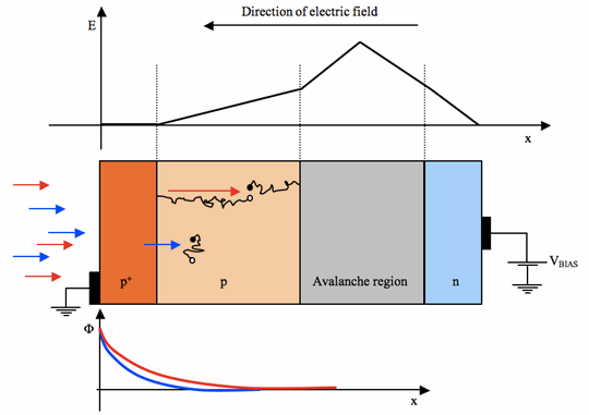
Figure 2. The structure and operation of an APD.
The light is incident on the p+ side. If the energy of light is greater than the band gap energy EG of the semiconductor used to manufacture the APD (typically silicon with EG = 1.1 eV), an intrinsic photoelectric effect can occur producing e-h pairs. Owing to its indirect band structure, the photon absorption process in silicon also involves a phonon — a quantized lattice vibration. The characteristic depth of photon absorption depends on the type of the semiconductor and the wavelength of light. The bottom panel of Figure 2 shows schematically that the flux Φ of "red" photons attenuates less with depth compared to the flux of "blue" photons. More specifically, photon flux Φ(λ, z) as a function of depth z is given by Equation 1.
Equation 1: Photon flux as a function of depth z.
Here, Φ(λ, 0) is the incident flux and α is the absorption coefficient, which depends on the type of the material and the wavelength of light, as shown in Figure 3.
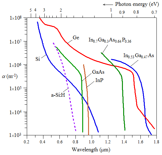
Figure 3. Absorption coefficient, α, as a function of wavelength of light (bottom abscissa) or energy (top abscissa) for several semiconductors.
Equation 1 shows that the production of e-h pairs decreases exponentially with depth; 63% of the incident photons are absorbed over a distance δ = 1/α, known as the penetration depth. In the case of silicon, δ is approximately 0.08 μm and 3 μm at λ = 400 nm and λ = 600 nm, respectively. As λ increases to the threshold value λth = hc/EG, α → 0 (or δ → ∞) and the material becomes progressively more transparent to the incoming radiation. However, as λ decreases, α → ∞ (or δ → 0) and the incoming radiation is absorbed near the surface. The dependence of α with respect to λ is a crucial parameter in the design of an APD.
If an e-h pair is produced in a heavily doped p+ region where the electric field is very weak, the pair is likely to recombine. For indirect band gap semiconductors like silicon, the recombination is mostly non-radiative and requires a phonon. The need for a phonon makes the lifetime of the pair longer than that for a pair produced in a direct band gap semiconductor (e.g., GaAs). Suppose that as a result of light illumination, an e-h pair forms close to or in the depletion region where the electric field is strong enough to separate the pair and make the electron move toward the n region and the hole toward the p+ region (see Figure 2). In the depletion region, the likelihood of e-h recombination is extremely small because the region lacks mobile charge carriers and, therefore, the injection produces an electrical signal in the circuit containing the detector. Light has been detected.
The quantum efficiency, η(λ), is defined as the ratio of the number of photo-generated e-h pairs per unit time, ne-h, that produce an electrical signal to the number of incident photons on a photo-sensitive surface per unit time, nλ.
Equation 2. Definition of quantum efficiency.
Figure 4 is an example quantum efficiency curve for a silicon APD manufactured by Hamamatsu.
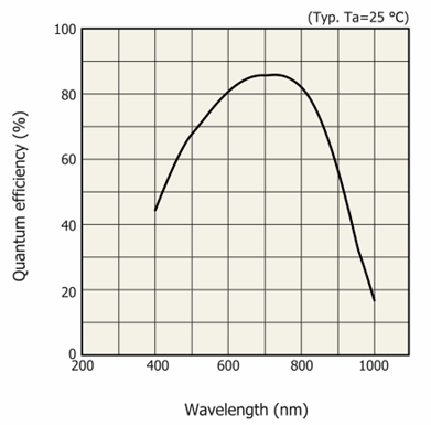
Figure 4. Quantum efficiency as a function of wavelength for Hamamatsu Si APD S10341.
The figure shows that for this particular APD, η(λ) has a broad maximum of approximately 85% for the wavelengths around 700 nm and that it declines more steeply for longer wavelengths than for shorter.
The rate at which the photo-produced charge carriers enter the depletion region is the photocurrent Iph and is given by Equation 3.
Equation 3. Photocurrent.
Here, P0 is the incident light power (assumed monochromatic light), e is the fundamental charge, h is Planck's constant, and c is the vacuum speed of light. The magnitude of the current flowing through the APD, IAPD, depends on Iph and on the strength of the electric field in the avalanche region. The field determines the degree of impact ionization in the avalanche region and, therefore, the gain M making IAPD = M x Iph. Because the strength of the electric field depends on VBIAS, a relationship exists between M and VBIAS. This relationship is one of the most important characteristics of an APD, and it is schematically shown in Figure 5.
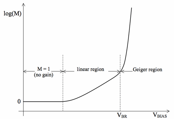
Figure 5. Gain versus reverse bias voltage for a hypothetical APD.
There are three distinct regions on the log(M) versus VBIAS plot. "No gain" or M = 1 is the characteristic of the first region. Here, IAPD = Iph and the APD operates as a photodiode. The electric field in the avalanche region is too weak to energize charge carriers to the minimum energy required for impact ionization of the lattice atoms.
In the linear region, log(M) is linearly proportional to VBIAS. Here, M > 1 because the charge carrier injected into the avalanche region gains enough kinetic energy to ionize a lattice atom. Therefore, one carrier (say an electron) becomes three after ionization: two electrons and one hole. These can now again be energized to cause further ionization events — an avalanche ensues. In the linear region, the avalanche eventually ceases; the electrons and holes produced by impact ionization are collected at the electrodes and their number is M — the gain.
The likelihood of impact ionization depends on the strength of the electric field. Let α and β be ionization coefficients representing the number of ionization events per unit length for electrons and holes, respectively. Figure 6 shows how α and β depend on the strength of the electric field (E) for several semiconductors. In the case of silicon (Si), α > β for any value of E implying that impact ionization due to an electron is more likely to occur than impact ionization due to a hole. Let k ≡ α/β (impact ionization ratio); the figure shows that k ≈ 0.01 for E ≈ 1.5 x 10⁵ V/cm and about 0.4 for E ≈ 6.0 x 10⁵ V/cm for Si, which means that the likelihood of impact ionization by electrons and holes converge with increasing strength of E.
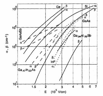
Figure 6. Ionization coefficients α (for electrons) and β (for holes) as a function of electric field strength for several semiconductors.
In the third region of Figure 5, the avalanche caused by injection of a single charge carrier does not stop—it is self-sustained. As a result, a current flows through the APD and its value depends on the overvoltage, ΔV. The steepness of the curve in this region implies that the magnitude of the current is very sensitive to ΔV. The strong electric field in the avalanche region maintains e-h plasma where both electrons and holes comparably ionize the lattice atoms (i.e., α ≈ β). In a steady state, the number of newly created pairs is equal to the number of pairs collected at the electrodes. This operation mode of an APD is known as Geiger mode. If it is desired to extinguish the avalanche, VBIAS must be reduced to at least VBR; doing so "quenches" the avalanche.
Section II: The physics of an MPPC pixel
Figure 7 depicts an equivalent circuit of a single MPPC pixel under bias conditions. The externally applied VBIAS is greater than VBR putting the APD—the section of the pixel delineated with the dashed rectangle—in Geiger mode. In series with the APD and VBIAS is RQ, the quenching resistor whose typical value is about 150 kΩ. When the switch is in the OFF position, the APD is in the "ready" state: the junction capacitance CJ is fully charged to the voltage VBIAS which is also the voltage VD across the terminals of the APD. The voltage VD creates an electric field in the depletion region that is strong enough to initiate a self-sustained avalanche if a charge carrier — electron or hole — is injected into the region. When the injection occurs, the switch instantly goes to the ON state and CJ begins to discharge through the resistor RS representing the combined series resistance of the depletion region — now containing plasma — and the resistance of the neutral regions of the APD. A typical value of RS is ~1 kΩ and that of CJ ~0.1 pF. The voltage on the discharging CJ approaches VBR with the characteristic time constant τ ~ RSCJ. For RS = 1 kΩ and CJ = 0.1 pF, τ ~ 100 ps.
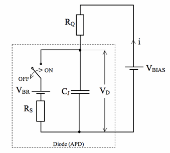
Figure 7. Equivalent circuit of an MPPC pixel externally biased by VBIAS. The region of the circuit delineated by the dashed rectangle represents an APD operating in Geiger mode. The switch is in the OFF position when the APD is in the "ready" state, while it goes to the ON state the instant a charge initiates an avalanche.
Applying Kirchhoff’s circuit rules, the voltage VD during the discharge decreases and approaches an asymptotic value given by Equation 4.
Equation 4. Asymptotic terminal voltage on the APD as the junction capacitance discharges.
For RQ >> RS, Equation 4 shows that VD tends to VBR. As VD decreases, the electric field in the depletion region decreases, eventually becoming too weak to maintain Geiger mode. The self-sustained avalanche stops — it’s been quenched by RQ — and the switch in the equivalent circuit (see Figure 7) goes to the OFF position. At this instant, CJ begins to charge from approximately VBR to VBIAS through RQ with the characteristic time constant τ ~ RQCJ. For RQ = 150 kΩ and CJ = 0.1 pF, τ ~ 15 ns. At the end of the charging process, the APD is in the "ready" state.
An external electronic detection circuit would be sensitive to the current flowing through the APD, which also flows through RQ and flows out of the positive terminal of VBIAS. Figure 8 depicts schematically how the current i varies with time as an MPPC pixel goes into and recovers from an avalanche.
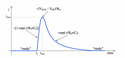
Figure 8. Current pulse generated by an MPPC pixel.
At any instant of time, i(t) = (VBIAS - VD)/RQ. When the pixel is in the "ready" state,VD = VBIAS and i(t) = 0. An injection of charge into the avalanche region occurs at the time ti. At this instant, CJ begins to discharge causing VD to decrease and i(t) to increase. The current i(t) tends to the maximum value imax ≈ (VBIAS - VBR)/RQ at the time tmax when RQ quenches the avalanche. Between ti and tmax, i(t) ~ imax[1 - exp(-t/RS x CJ)]. For times greater than tmax, CJ charges through RQ, and the current decreases as i(t) ~ imaxexp(-t/RQCJ). Because RSCJ << RQCJ, the current rises more steeply before tmax then it falls off after tmax. Thus, the output current pulse has the characteristic asymmetric shape.
An integral of i(t) with respect to time from ti to infinity is the area under this curve, which equals the net charge Q produced in the avalanche. A detailed analysis yields the following.
Equation 5. Net charge produced by an avalanche.
Since the charge Q is due to a single charge injected into the avalanche region, the gain M for this process can be defined by Equation 6.
Equation 6. Definition of gain.
For a fully depleted junction, CJ is constant with respect to the applied voltage and, thus, Equation 5 shows that M is linearly proportional to VBIAS - VBR = ΔV. The typical values of M range from 105 to 106. If more than one pixel developed an avalanche at the time ti, the total charge generated by an MPPC is the following.
Equation 7. Output charge from an MPPC when Nf pixels "fired."
Here, Nf is the number of pixels that nearly simultaneously "fired" or developed avalanches.
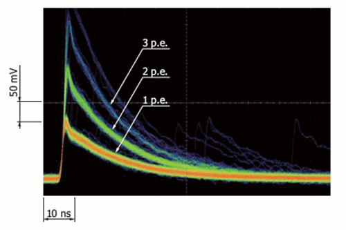
Figure 9. Waveforms analogous to the one depicted in Figure 8 for Hamamatsu S12571-050C MPPC producing signal when 1, 2, 3, … pixels fired simultaneously in response to light. Note a few 1 p.e. waveforms that are lagging in time to the main events. The waveforms are for gain M = 1.25 x 10⁶ and 120x linear amplifier.
Figure 9 shows oscilloscope traces of waveforms (analogous to the one schematically illustrated in Figure 8) produced by an MPPC in response to low-intensity light. From bottom up, the waveforms correspond to the outputs characterized by an increasing number of simultaneously "fired" independent pixels. The waveforms labeled 1 p.e. are for the outputs where only one pixel has fired in response to light. Note that if two or more photons were to be simultaneously absorbed by this same pixel, the output waveform would have been the same. Similarly, the waveforms labeled 2 p.e. are for two pixels firing simultaneously. To obtain these cumulative waveforms, the oscilloscope is set to the persistence mode; thus, the color in the figure corresponds to the frequency with which the events have occurred. There is a clear demarcation between waveforms labeled 1 p.e., 2 p.e., 3 p.e., etc. The 1 p.e. waveforms were the most common (orange color), whereas the 3 p.e. events were least common among the three labeled sets. Note that there are a few 1 p.e. waveforms that are lagging in time to the main events. They can be generated in three ways: dark noise, afterpulsing, and cross-talk.
Dark noise pulses occur randomly and are due to thermally generated charge carriers reaching the avalanche region. If a pixel is in the "ready" state, the ensuing "dark" pulse is indistinguishable from one due to photon absorption. Such a pulse would be labeled 1 p.e. in Figure 9. If, however, the pixel is recovering from a primary avalanche, the "dark" pulse lags in time to the primary pulse but is not correlated with it.
The pulses due to afterpulsing and cross-talk are correlated to the primary avalanche, which can be due to photon absorption or dark noise. Afterpulsing occurs when lattice defects trap charge during an avalanche and then release the charge while the pixel recovers. The release triggers a correlated secondary avalanche whose gain M depends on ΔV at the time of release. Cross-talk occurs when a primary avalanche in a pixel produces photons with energy greater than the band gap energy. If the same pixel reabsorbs the photon, the resulting secondary pulse would look like an afterpulse. However, if a nearby pixel absorbs the photon, the secondary correlated avalanche may be close enough in time to the primary that the resulting waveform would be labeled 2 p.e. in Figure 9. Section IV below discusses in greater detail dark noise, afterpulsing, and cross-talk.
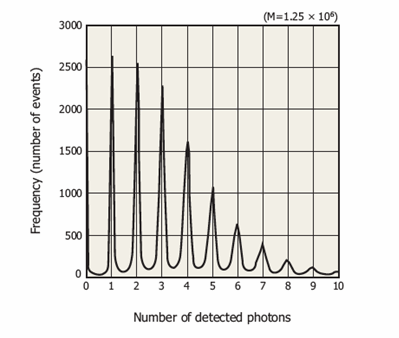
Figure 10. Output charge spectrum for waveforms in Figure 9. Although the horizontal axis corresponds to the output charge, there is a linear mapping between this quantity and the number of detected photons, which is shown instead.
Integrating a waveform with respect to time gives the net output charge for the event. The amount of output charge is linearly proportional to the number of fired pixels, which, in turn, is proportional to the number of simultaneously absorbed photons. Therefore, information in Figure 9 after integrating each waveform can be expressed in the form of a histogram; Figure 10 is an example of such a histogram.
Section III: Architecture of an MPPC detector
Figures 11 (side view) and 12 (top view) illustrate a common architecture of an MPPC array. The accompanying Figure 13 shows schematically the distribution of the dopant ions or space charge (left panel) and the resulting strength of the electric field (right panel) as a function of depth. Following the direction of light — red arrows in the leftmost pixel of Figure 11 — they first encountered a very thin (~ 10 nm) anti-reflection coating. The coating improves light transmittance to the next layer, a transparent silicon dioxide, which acts as the window and an insulation between the metal contacts above and semiconductor below. A typical thickness of the insulation is ~0.15 μm. Further below, there is a heavily doped n+ layer, which is connected to the metal contact above through the quenching resistor RQ. The resistor is made of polysilicon. The thickness of the n+ layer ranges from 0.1 μm to 1.5 μm. Immediately below, there is a heavily doped p+ layer with a typical thickness of a few μm. A depletion region where conditions for an avalanche can exist forms at the junction of the n+ and p+ layers. The width of the depletion region depends on the applied VBIAS; for Geiger mode operation, it is ~1 μm.
In this "reach through" architecture, a photon creates an e-h pair in the thick (~300 μm) and lightly doped π layer. As Figure 13 shows, the electric field in this region can separate the pair and direct the electron towards the depletion region and the hole toward the substrate — a thin (~3 μm) p+ layer that makes an ohmic contact with the metal contact below. Upon reaching the depletion region, the electron can initiate an avalanche, while the hole upon reaching the metal contact cancels with an electron coming from the metal contact.
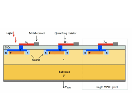
Figure 11. Architecture of a silicon photomultiplier (side view). The depicted structure of a single pixel is known as "reach-through" structure, popular with manufacturers. Please note that this figure depicts a typical structure of a silicon photomultiplier and is included here solely for explanatory purposes. It does not correspond to the actual structure of the Hamamatsu product.
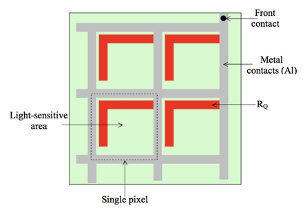
Figure 12. Architecture of an MPPC (top view). Please note this figure depicts a typical structure of a silicon photomultiplier and is included here solely for explanatory purposes. It does not correspond to the actual structure of the Hamamatsu product.
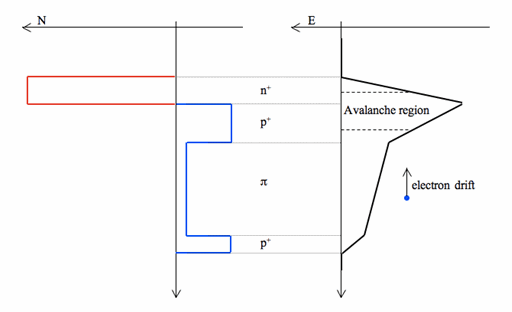
Figure 13. Schematic distribution of dopant ions (left) and the resulting electric field (right) for a pixel in the structure shown in Figures 11 and 12.
The area of a pixel that is sensitive to light is smaller than its geometrical area. The ratio of the two is known as the fill factor, Fg. The values of Fg range from about 30% to 80%. An MPPC is a square array (circular arrays are also manufactured) of pixels with the number of pixels ranging from 100 (10 x 10) to 14400 (120 x 120). The typical geometrical areas of the pixels (in μm2) are 25 x 25, 50 x 50, and 100 x 100. Multiplying the geometrical area of a pixel by the number of pixels yields the total geometrical area of the detector; two values are typical: 1 x 1 mm2 and 3 x 3 mm2. Multiplying the geometrical area by the appropriate fill factor gives the total light-sensitive area of the detector.
Section IV: Performance characteristics of an MPPC
Dark noise
If a thermal fluctuation creates an e-h pair in the depletion region of an MPPC pixel, a charge carrier can enter the avalanche region and trigger an avalanche that is indistinguishable from one resulting from photon absorption. A less likely but still possible scenario is when a pair is thermally produced in the avalanche region itself. In either case, the resulting pulse is referred to as dark noise. The occurrence of dark noise is random in time and uncorrelated to the pulses resulting from photon absorption. The rate of dark noise, however, will depend on overvoltage, temperature, pixel size, and quality of the material semiconductor.
Vacheret et al. (2011) performed a series of experiments in order to characterize the optical and electrical properties of a T2K MPPC; this detector is a customized version of the Hamamatsu S10362-11-050C. The former is a 26 x 26 array of 50 x 50 μm2 pixels with nine pixels replaced with a lead giving 667 active pixels. The latter is a 20 x 20 array of pixels of the same size. The study reports how dark noise rate varies with overvoltage ΔV (Figure 14) and temperature (Figure 15).
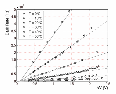
Figure 14. Dark noise rate as a function of overvoltage for several temperatures. Adapted from Vacheret et al. (2011).
Figure 14 shows that dark noise rate increases nearly linearly with increasing ΔV regardless of temperature, but the rate of the increase (slope) increases with temperature (equation 4 in Vecheret et al. (2011) gives the form of the function used for fitting the data). At a given ΔV, the dark noise rate increases with temperature.
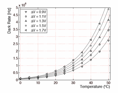
Figure 15. Dark noise rate as a function of temperature for several values of overvoltage. Adapted from Vacheret et al. (2011).
The dark noise rate increases nearly exponentially with temperature regardless of ΔV as shown in Figure 15. At a given temperature, the rate is higher for larger ΔV. The study also finds that the dark noise rates varied significantly, about 20%, among the 17,686 MPPCs tested at T = 20 °C and ΔV = 1.0 V.
Dark noise also depends on the pixel size. Figure 16 shows dark noise as a function of ΔV for six MPPCs listed in the insert box. From top to bottom, the first four are from Hamamatsu; by the company's naming convention, the third set of digits in the part number, e.g., 025 or 100, represents pixel size, e.g., 25 x 25 μm2 or 100 x 100 μm2. The bottom two MPPCs are from SensL, and each one has a pixel size of 20 x 20 μm2. Assuming that the MPPCs from Hamamatsu have similar wafer quality, the figure implies that for a given ΔV, the dark noise rate increases with the pixel size; however, the ratio of the dark noises for a given ΔV does not equal the ratio of the pixel sizes. Although the pixels in the MPPCs from SensL have the smallest size, the dark noise in them is not, which could be due to a lower quality of the semiconductor wafer.
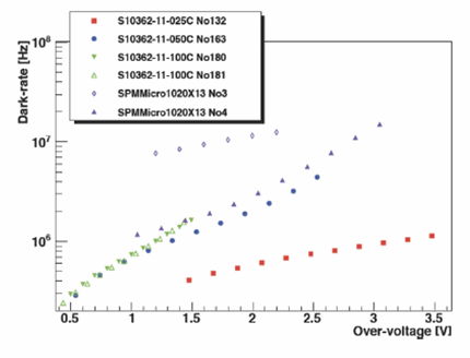
Figure 16. Dark noise rate as a function of temperature for several values of overvoltage. Adapted from Garutti (2011).
Afterpulsing
Afterpulsing occurs when a secondary avalanche forms in a pixel that is recovering from a photon- or dark-noise-induced primary avalanche. The secondary avalanche is due to the release of trapped charge — electrons — at some time τS after the primary avalanche starts. Figure 17 shows a "forest" of waveforms due to afterpulsing that exhibit a wide range of values of τS (from a few ns to many tens of ns). Note that when an afterpulse waveform starts, its vertical coordinate is the vertical coordinate of the primary waveform at this instant.
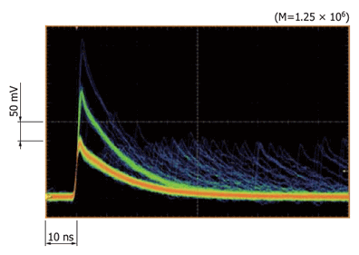
Figure 17. A "forest" of waveforms due to afterpulsing lagging the primary waveforms. The time delays between the primary and secondary waveforms range from a few ns to many tens of ns.
The amount of charge generated in an afterpulse is proportional to the area under the afterpulse (or secondary) waveform with respect to the primary waveform. The amount of charge increases with τS, and for sufficiently long τS when the pixel completely recovers, the afterpulse waveform becomes indistinguishable from the 1 p.e. waveform. In this case, afterpulsing erroneously increases the number of 1 p.e. events in photon counting, which translates into an erroneous increase in photon detection efficiency (PDE; described in greater detail below). Afterpulsing also increases the recovery time of the fired pixel, which degrades the time resolution characteristic of an MPPC.
The likelihood of afterpulsing increases with increasing ΔV because the stronger electric field in the avalanche region more effectively dislodges the trapped charges and also increases avalanche probability. Eckert et al. (2010) measured the probability of afterpulsing as a function of ΔV for three Hamamatsu MPPCs, and Figure 18 shows the results. The MPPCs belong to the same family differing only in pixel size (025C being the smallest and 100C the largest). For all three MPPCs, the probability increases with ΔV but the increase is steepest for the MPPC with the largest pixel size. In addition, for a given ΔV, the MPPC with the largest pixel size has the largest probability of afterpulsing.
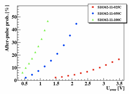
Figure 18. Afterpulsing probability as a function of overvoltage. Adapted from Eckert et al. (2010).
Cross-talk
Cross-talk occurs when an avalanche in a pixel generates photons energetic enough to initiate a correlated avalanche in neighboring pixels, as shown schematically in Figure 19. Even though silicon is an indirect band gap semiconductor, emission of light does occur as carriers pass the p-n junction — an effect first observed by Newman et al. (1955). Lacaita et al. (1993) shows that about 3 x 10⁻⁵ photons are emitted with energy greater than 1.14 eV per charge carrier crossing the junction. Assuming a gain of 106, a typical avalanche emits ~30 photons capable of causing cross-talk.
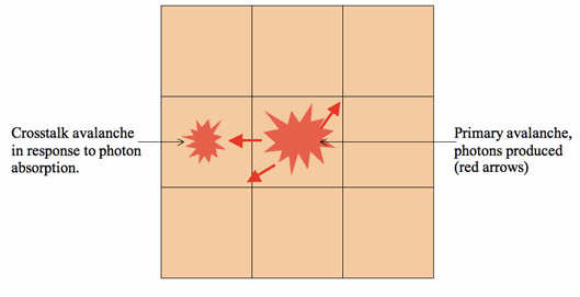
Figure 19. The mechanism of cross-talk. An avalanche in the central pixel produces photons energetic enough so that a correlated avalanche in a neighboring pixel can occur as a result of the photon absorption.
To cause cross-talk, a photon must create an e-h pair in the region of a neighboring pixel where one or both of the charge carriers can be injected into the avalanche region. Since the emission of photons is isotropic, this event has a small probability. Moreover, some fraction of the photons will be absorbed in the pixel from which they were emitted, possibly causing afterpulsing in the pixel. The time for a photon to cross a pixel of size d is tc ≈ nd/c, where n is the index of refraction of the material. For silicon n = 3.96; thus, for d = 25 μm, tc = 0.33 ps. This crossing time is much shorter than pixel recovery time (~15 ns) and, therefore, the MPPC would output at least a 2 p.e. waveform in response to a single external photon. The value of tc scales linearly with d, but even for a 100 μm pixel, it is still small compared to pixel recovery time. Nevertheless, the probability of cross-talk decreases with pixel size because the emitted photon has an increasing chance of being reabsorbed in the same pixel.
Eckert et al. (2010) reports measurements of the probability of cross-talk as a function of gain for three MPPCs manufactured by Hamamatsu and one by SensL. Figure 20 displays the results. Since the gain is proportional to the overvoltage ΔV, the figure can also be interpreted as the probability of cross-talk versus ΔV. For all of the tested MPPCs, the probability increases with gain (ΔV) because the number of charge carriers crossing the junction increases which, in turn, increases the number of emitted photons. Increasing ΔV also increases the probability of avalanche. For a given ΔV, the probability of cross-talk decreases with increasing pixel size, as can be seen for the MPPCs manufactured by Hamamatsu.
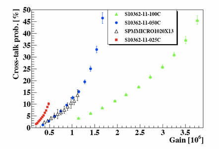
Figure 20. Probability of cross-talk as a function of gain for three MPPCs manufactured by Hamamatsu (S10362 series) and one manufactured by SensL. Adapted from Eckert et al. (2010).
Akil et al. (1999) investigates the mechanisms for light emission from, among others, a silicon p-n junction operating in an avalanche mode. The study concludes that three distinct processes contribute to the observed spectrum, which is shown in Figure 21. Indirect interband recombination between electrons and holes in strong electric fields is primarily responsible for the emission below the ~2 eV peak in the spectrum. Bremsstrahlung radiation due to scattering of conduction electrons from positive ions is mainly responsible for the shape of the spectrum between ~2 eV and ~2.3 eV. Interband recombination between "hot" conduction electrons and holes describes the emission of radiation above ~2.3 eV.
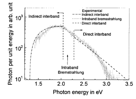
Figure 21. Emission spectrum from an avalanche silicon p-n junction. A model combining the three listed emission processes is fitted to the spectrum. Adapted from Akil et al. (1999).
Temperature dependence
In a constant temperature environment, the overvoltage ΔV applied to an MPPC determines its operational characteristics such as gain and PDE. Because temperature is an important parameter affecting the opto-electrical characteristics of a p-n junction such as the width of the depletion region, the breakdown voltage, band-gap energy, resistivity, and more, the operation of an MPPC will be strongly affected by this parameter. One example of the dependence is the recovery time of a pixel from avalanche. The characteristic time of the recovery is the RC time constant determined by the values of the junction capacitance CJ and of the quenching resistor RQ. For a given ΔV, temperature affects the width of the depletion region and, thus, CJ. It also affects the resistance of the polysilicon resistor — the quenching resistor — RQ. Thus, the product of these two quantities can also change with temperature affecting the recovery time.
Dinu et al. (2010) investigates how temperature affects the operational characteristics of two Hamamatsu MPPCs: S10362-11-050U-3 and S10362-33-050C-329. Both have 50 μm x 50 μm pixels and total areas of 1 x 1 mm2 and 3 x 3 mm2, respectively. The temperatures are in two ranges: -110 °C to -50 °C and 0 °C to 38 °C. Below is a summary of the main results from the study for S10362-11-050U-3.
Figure 22 shows the dependence of the gain on the bias voltage parameterized by temperature. For each temperature, the relationship is linear and the horizontal-intercept (where there is no gain) gives the breakdown voltage. Plotting the breakdown voltage as a function of temperature shows a linear relationship (Fig 2 in the study) as well. Therefore, for a given bias voltage, the gain decreases with increasing temperature.
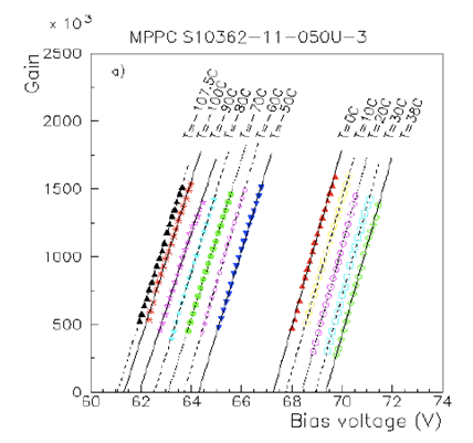
Figure 22. Gain vs. bias voltage parameterized by temperature. Adapted from Dinu et al. (2010).
As the temperature increases, the Boltzmann distribution implies an increasing fraction of electrons in the conduction band and, thus, a decreasing resistivity of the semiconductor. Because the quenching resistor is made from polysilicon, RQ will decrease with increasing temperature. The junction capacitance, CJ, also varies with temperature. With zero bias, CJ ∝ 1/√Vbi, where Vbi is the p-n junction built-in voltage. Because Vbi decreases with temperature, CJ increases with temperature. Figure 23 confirms both behaviors: the red triangles correspond to the resistance of RQ and the blue circles correspond to the capacitance of CJ. The product of the two curves does not yield a horizontal line and, thus, the RC time constant itself is a function of temperature affecting the recovery time, as shown in Figure 24.
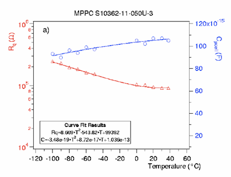
Figure 23. Temperature dependence of the quenching resistance (red) and junction capacitance (blue). Adapted from Dinu et al. (2010).
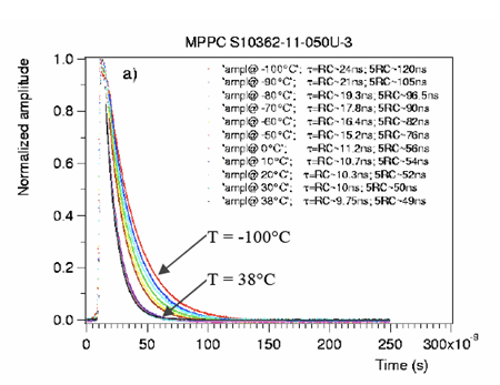
Figure 24. Waveform shapes as a function of temperature. Adapted from Dinu et al. (2010).
Section V: Optical and electrical characteristics of an MPPC
Photon detection efficiency
The photon detection efficiency is the percentage of the incident photons on the geometrical area of an MPPC that is detected.
Equation 8. Photon detection efficiency is a product of quantum efficiency, fill factor, and probability of an avalanche.
In Equation 8, η is the quantum efficiency defined by Equation 2, Fg is the fill factor, and Pa is the combined probability of electrons and holes initiating Geiger mode avalanche. Because η is a function of wavelength and Pa is a function of VBIAS, PDE depends on both wavelength and VBIAS. Eckert et al. (2010) performed a series of experiments designed, among others, to measure an absolute PDE and its dependence on overvoltage and wavelength for several MPPCs manufactured by Hamamatsu. Figure 25 is an example of the results.
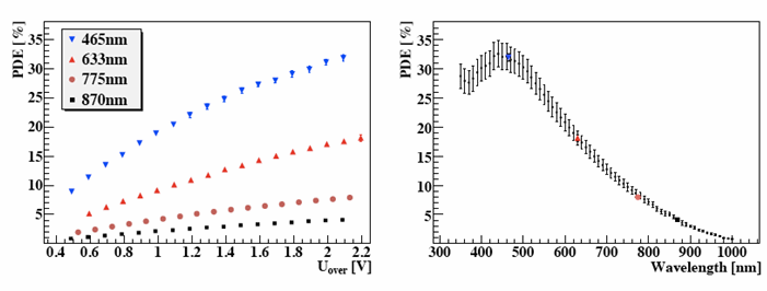
Figure 25. PDE as a function of overvoltage (left) and wavelength (right) for Hamamatsu S10362-11-050C MPPC at room temperature (25 ± 1.5 °C). Reproduced from Eckert et al. (2010).
The left panel of the figure shows how the PDE depends on overvoltage ΔV for four wavelengths (465 nm, 633 nm, 775 nm, and 870 nm), and the right panel shows how the PDE depends on wavelength for ΔV = 2.15 ± 0.05 V. For each wavelength, the PDE increases monotonically with ΔV, and the rate of the increase depends on wavelength: it is greatest for λ = 465 nm. At a given ΔV of the experimental range (~0.5 V to 2.2 V), the absolute PDE increases with decreasing wavelength. However, the right panel suggests that the PDE reaches maximum at λ ≈ 440 nm and declines with further increase of wavelength. Hamamatsu provides a plot of the PDE versus wavelength for the S10362-11-050C MPPC, which is shown in Figure 26. The measurements are for ΔV = 1.5 V.
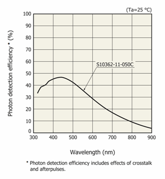
Figure 26. PDE versus wavelength for the S10362-11-050C MPPC provided by the manufacturer, Hamamatsu Photonics K.K. The measurements are for ΔV = 1.5 V.
Comparing Figures 25 and 26 shows that the shapes of the curves are similar but that the magnitude of the PDE in the latter plot is greater at all wavelengths, even though the measurements are for ΔV = 1.5 V. As noted by Eckert et al. (2010), this substantial discrepancy in the two plots is likely due to the methodology of the measurements. Eckert et al. (2010) exclude the effects of cross-talk and afterpulsing, whereas Hamamatsu does not (as noted on the graph). Recently, Hamamatsu has released a new and improved line of MPPCs which, compared to the older line, have greatly reduced cross-talk and afterpulsing. In addition, Hamamatsu has changed the methodology of measuring PDE versus wavelength that now excludes cross-talk and afterpulsing. MPPC S12571-050C is the new and improved version of the S10362-11-050C, and Figure 27 shows how its PDE depends on wavelength.
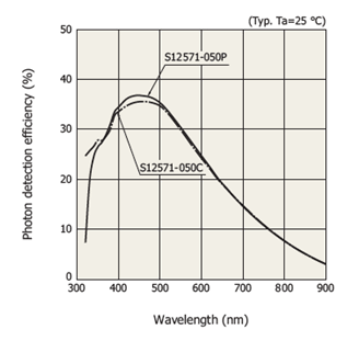
Figure 27. PDE versus wavelength for two Hamamatsu MPPCs. The measured PDE excludes effects due to cross-talk and afterpulsing. The measurements are for the overvoltage of 2.6 V.
Dynamic range
An ideal photodetector would produce an electrical output that is linearly proportional to the entire range of input light levels. This property, referred to as linearity, is a highly desirable feature in practical photodetectors, but it is never realized for all signal levels. Noise inherent to a detector limits the lowest detectable light level, whereas a variety of phenomena that are unique to the detector, cause a non-linear behavior and eventually saturation. Dynamic range is a ratio of the maximum light level that a detector can detect without saturation or deviation from linearity and of the minimum detectable light level, which would produce S/N = 1.
Suppose that an MPPC with N pixels is diffusely illuminated by an "instantaneous" pulse of light containing Nγ photons. The MPPC operates at an overvoltage ΔV, which determines its PDE. Renker and Lorenz (2009) find that the number of fired pixels Nf as a function of Nγ is well modeled by Equation 9.
Equation 9. Empirical relationship between the number of fired pixels and a number of incident photons for an MPPC with N pixels.
Since e-x ≈ 1 - x for x << 1, Equation 9 implies that if Nγ·PDE << N, Nf ≈ Nγ·PDE — the number of fired pixels is linearly proportional to the number of photons. However, if the number of photons per pulse increases or, alternatively, if the number of pixels decreases, so that the exponent is no longer small, Nf is no longer linearly proportional to Nγ·PDE, or the upper limit of the dynamic range has been reached. Suppose that an MPPC has 100 pixels and a PDE of 40%; Equation 9 implies the output of the MPPC would deviate from linearity by 1% for 5 photons and by 10% for 54 photons per pulse. Increasing the number of pixels to 14,400 keeping the PDE the same, 1% and 10% deviations from linearity occur for 700 and 7,750 photons per pulse, respectively. Taking 1% to be the maximum tolerable deviation from linearity, increasing the number of pixels has increased the dynamic range by about 140 assuming that the lowest detectable signal is one photon. The increase in the dynamic range is approximately equal to the factor by which the number of pixels has increased. Equation 9 also implies that increasing PDE can actually reduce the dynamic range. Assuming a theoretical value for PDE of 0.8, the deviation from linearity for 700 photons in the last example would be 2%. In contrast, reducing PDE to 0.2 would improve linearity by 0.5%.
Gruber et al. (2014) measured the number of fired pixels as a function of Nγ·PDE ≡ Nseed for several MPPCs with different number of pixels using laser pulses (λ = 404 nm) of 32 ps duration and 20 kHz repetition rate and compared the measurements with the predictions of the model given by Equation 9. Figure 28 (top two rows of panels from Figure 5 in the study) shows the results for the MPPCs manufactured by Hamamatsu: S10362-11-100U (top row of panels) and S10362-11-050U (bottom row of panels).
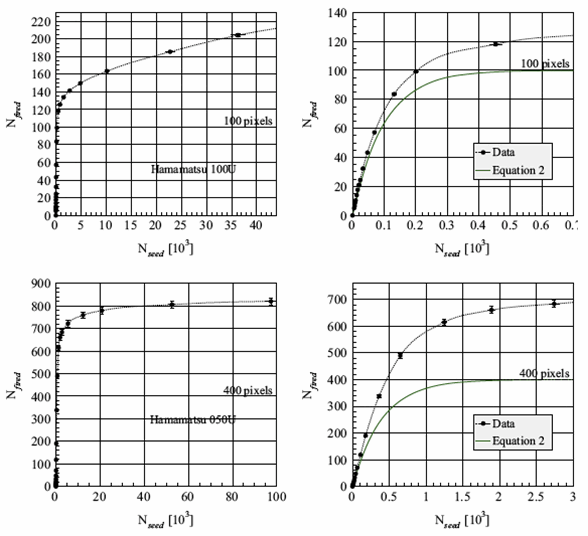
Figure 28. Number of fired pixels Nfired as a function of the number of seed photons Nseed for Hamamatsu S10362-11-100U (top) and S10362-11-050U (bottom) MPPCs. Note different scales on the horizontal axes. The curves drawn in green in the figures on the right are model predictions given by Equation 9. The horizontal lines labeled "100 pixels" and "400 pixels" are saturation levels given by the model and equal to the number of pixels in the detector.
The panels on the left are for "high" and those on the right are for "low-to-medium" light intensities (note different scales on the horizontal axes). The horizontal lines labeled either 100 pixels (top row) or 400 pixels (bottom row) represent the expected saturation levels (equal to the number of pixels in the detector) predicted by the model in Equation 9 (or by the same Equation 2 in the study). In the panels on the right, the measured values of Nf (or Nfired) are compared to the predictions of the model (green line). The measured values of Nf are higher than the model values and, most surprisingly, can exceed the number of pixels in the detector or the saturation level. Gruber et al. (2014) discusses several possible explanations for this "over saturation" but concludes that none of the explanations is satisfactory and warns that our current understanding of how an MPPC operates may be incomplete.
Time characteristics
The time elapsed between the instant when a single photon strikes a photodetector and the instant when the photodetector produces an electrical output is called the single photon response time (SPRT). In the case of an ideal photodetector, repeated strikes by single photons would result in identical values of SPRT. In a practical detector, the values of SPRT differ. The spread of theses values implies a limit in the ability of the detector to resolve in time distinct photonic or particle events, e.g., in coincidence counting. Single photon timing resolution (SPTR) is a measure of the spread of the SPRT values, and it is one of the more important characteristics of a detector.
The origin of SPTR in an MPPC has several reasons. 1) The exact locations in the pixel where the incident photons create e-h pairs differ due to the stochastic nature of the photoelectric effect. 2) The drift times of charge carriers from the points of their creation to the avalanche region in the pixel differ even if the points of creation were to be the same. The drift times vary because the carriers form with different initial velocities and because they have different histories of scattering events along their paths to the avalanche region. 3) The times when avalanches are triggered by entering charge carriers into the depletion region vary because: a) the velocities of entering charge carriers differ; b) the strength of the electric field in the avalanche region fluctuates; c) the stochastic nature of the triggering of an avalanche, expressed as a probability. 4) Time constants of pixels vary because of differences, albeit small, in the values of RS, RQ, and CJ. 5) The paths for the output current signals to propagate between the pixels and the common output signal line vary due to the geometrical structure of an MPPC. The importance of the aforementioned factors affecting SPTR can depend on quantities such as, e.g., ΔV, wavelength of light, temperature, or number and size of pixels, SPTR itself can exhibit a dependence on these quantities.
Recently, Puill et al. (2012) has investigated how overvoltage, temperature, and wavelength of light affect SPTR of several MPPCs. The work finds that SPTR improves considerably with ΔV as shown in Figure 29 (Figure 3 in the original study). The plotted data are for 1 mm2 MPPCs (listed in the figure insert) at 20 °C using light with λ = 467 nm. Although SPTR improves with ΔV, the dark count rate also increases making detection of a single photon harder. The figure shows that for ΔV = 1 V, the best SPTR ≈ 200 ps.
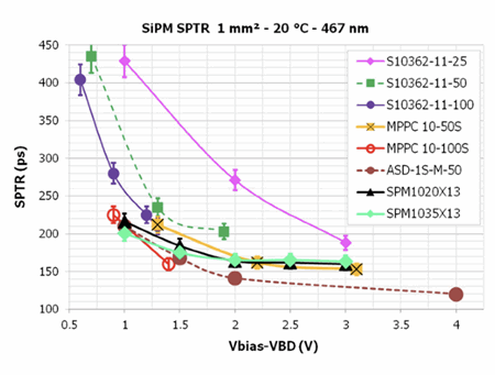
Figure 29. Single photon timing resolution as a function of overvoltage for several MPPCs. Adapted from Puill et al. (2012).
Puill et al. (2012) also finds that lowering the temperature from 20 °C to 0 °C slightly improves SPTR (see Figure 4 in the original study) and increasing the wavelength can slightly improve or worsen SPTR depending on the detector.
Summary
This paper reviews the physics and operation of a Multi-Pixel Photon Counter. The key findings and conclusions from the review are as follows:
- A single pixel in an MPPC consists of an APD operating in Geiger mode connected in series with a quenching resistor.
- An MPPC is an array of pixels connected together in parallel. The pixels have a common power source and common output.
- An MPPC can be thought of as a solid-state analog to a PMT and, thus, its utility as a photodetector is in the very low light level regime.
- Overvoltage, the difference between the external bias voltage and the breakdown voltage of the APD, is the most important parameter affecting the performance of an MPPC such as gain and noise level.
- Operation of an MPPC is sensitive to temperature.
- Three phenomena contribute to noise in an MPPC: thermally induced dark pulses, afterpulses, and cross-talk.
- Photon detection efficiency is the most important opto-electrical characteristic of an MPPC. Its value depends on overvoltage and wavelength of light.
- The dynamic range of an MPPC increases with the number of pixels.
- Single photon timing resolution of an MPPC is on the order of a few hundreds ps and decreases with increasing overvoltage.
References
- N. Akil, S. E. Kerns, D. V. Kerns, Jr., A. Hoffmann, and Jean-Pierre Charles, "A Multimechanism Model for Photon Generation by Silicon Junctions in Avalanche Breakdown," IEEE Trans. on Electron Devices vol. 46, No. 5 (1999): 1022-1028.
- N. Dinu, C. Bazin., V. Chaumat, et. al., "Temperature and Bias Voltage Dependence of the MPPC Detectors," IEEE Nucl. Sci. Symp. Conference Record (2010).
- P. Eckert, H.C. Schultz-Coulon, W. Shen, R. Stamen and A. Tadday, "Characterization studies of silicon photomultipliers," Nucl. Instrum. and Meth. A 620 (2010): 217-26.
- E. Garutti, "Silicon photomultipliers for high energy physics detectors," Journal of Instrumentation Vol. 6 (2011).
- L. Gruber, S. E. Brunner, J. Marton, and K. Suzuki, "Over saturation behavior of SiPMs at high photon exposure," Nucl. Instrum. and Meth. A 737 (2014): 11-18.
- A. L. Lacaita, F. Zappa, S. Bigliardi, M. Manfredi, "On the Bremsstranhlung origin of hot carrier induced photons in silicon devices," IEEE Trans. Nucl. Dev., vol. 40, No. 3 (1993): 577-582.
- R. Newman, "Visible light from a silicon p-n junction," Phys. Rev., vol. 100, no. 2 (1995): 700-703.
- V. Puill, C. Bazin, D. Breton, L. Burmistrov, V. Chaumat, N. Dinu, J. Maalmi, J. F. Vagnucci, A. Stocchi, "Single photoelectron timing resolution of SiPM as a function of the bias voltage, the wavelength and the temperature," Nucl. Instrum. and Meth. A 695 (2012): 354-358.
- D. Renker, E. Lorenz, Journal of Instrumentation 4 (2009) 04004.
- A. Vacheret et al., "Characterization and simulation of the response of Multi-Pixel Photon Counters to low light levels," Nucl. Instrum. and Meth. A 656 (2011): 69-83.
- Confirmation
-
It looks like you're in the . If this is not your location, please select the correct region or country below.
You're headed to Hamamatsu Photonics website for US (English). If you want to view an other country's site, the optimized information will be provided by selecting options below.
In order to use this website comfortably, we use cookies. For cookie details please see our cookie policy.
- Cookie Policy
-
This website or its third-party tools use cookies, which are necessary to its functioning and required to achieve the purposes illustrated in this cookie policy. By closing the cookie warning banner, scrolling the page, clicking a link or continuing to browse otherwise, you agree to the use of cookies.
Hamamatsu uses cookies in order to enhance your experience on our website and ensure that our website functions.
You can visit this page at any time to learn more about cookies, get the most up to date information on how we use cookies and manage your cookie settings. We will not use cookies for any purpose other than the ones stated, but please note that we reserve the right to update our cookies.
1. What are cookies?
For modern websites to work according to visitor’s expectations, they need to collect certain basic information about visitors. To do this, a site will create small text files which are placed on visitor’s devices (computer or mobile) - these files are known as cookies when you access a website. Cookies are used in order to make websites function and work efficiently. Cookies are uniquely assigned to each visitor and can only be read by a web server in the domain that issued the cookie to the visitor. Cookies cannot be used to run programs or deliver viruses to a visitor’s device.
Cookies do various jobs which make the visitor’s experience of the internet much smoother and more interactive. For instance, cookies are used to remember the visitor’s preferences on sites they visit often, to remember language preference and to help navigate between pages more efficiently. Much, though not all, of the data collected is anonymous, though some of it is designed to detect browsing patterns and approximate geographical location to improve the visitor experience.
Certain type of cookies may require the data subject’s consent before storing them on the computer.
2. What are the different types of cookies?
This website uses two types of cookies:
- First party cookies. For our website, the first party cookies are controlled and maintained by Hamamatsu. No other parties have access to these cookies.
- Third party cookies. These cookies are implemented by organizations outside Hamamatsu. We do not have access to the data in these cookies, but we use these cookies to improve the overall website experience.
3. How do we use cookies?
This website uses cookies for following purposes:
- Certain cookies are necessary for our website to function. These are strictly necessary cookies and are required to enable website access, support navigation or provide relevant content. These cookies direct you to the correct region or country, and support security and ecommerce. Strictly necessary cookies also enforce your privacy preferences. Without these strictly necessary cookies, much of our website will not function.
- Analytics cookies are used to track website usage. This data enables us to improve our website usability, performance and website administration. In our analytics cookies, we do not store any personal identifying information.
- Functionality cookies. These are used to recognize you when you return to our website. This enables us to personalize our content for you, greet you by name and remember your preferences (for example, your choice of language or region).
- These cookies record your visit to our website, the pages you have visited and the links you have followed. We will use this information to make our website and the advertising displayed on it more relevant to your interests. We may also share this information with third parties for this purpose.
Cookies help us help you. Through the use of cookies, we learn what is important to our visitors and we develop and enhance website content and functionality to support your experience. Much of our website can be accessed if cookies are disabled, however certain website functions may not work. And, we believe your current and future visits will be enhanced if cookies are enabled.
4. Which cookies do we use?
There are two ways to manage cookie preferences.
- You can set your cookie preferences on your device or in your browser.
- You can set your cookie preferences at the website level.
If you don’t want to receive cookies, you can modify your browser so that it notifies you when cookies are sent to it or you can refuse cookies altogether. You can also delete cookies that have already been set.
If you wish to restrict or block web browser cookies which are set on your device then you can do this through your browser settings; the Help function within your browser should tell you how. Alternatively, you may wish to visit www.aboutcookies.org, which contains comprehensive information on how to do this on a wide variety of desktop browsers.
5. What are Internet tags and how do we use them with cookies?
Occasionally, we may use internet tags (also known as action tags, single-pixel GIFs, clear GIFs, invisible GIFs and 1-by-1 GIFs) at this site and may deploy these tags/cookies through a third-party advertising partner or a web analytical service partner which may be located and store the respective information (including your IP-address) in a foreign country. These tags/cookies are placed on both online advertisements that bring users to this site and on different pages of this site. We use this technology to measure the visitors' responses to our sites and the effectiveness of our advertising campaigns (including how many times a page is opened and which information is consulted) as well as to evaluate your use of this website. The third-party partner or the web analytical service partner may be able to collect data about visitors to our and other sites because of these internet tags/cookies, may compose reports regarding the website’s activity for us and may provide further services which are related to the use of the website and the internet. They may provide such information to other parties if there is a legal requirement that they do so, or if they hire the other parties to process information on their behalf.
If you would like more information about web tags and cookies associated with on-line advertising or to opt-out of third-party collection of this information, please visit the Network Advertising Initiative website http://www.networkadvertising.org.
6. Analytics and Advertisement Cookies
We use third-party cookies (such as Google Analytics) to track visitors on our website, to get reports about how visitors use the website and to inform, optimize and serve ads based on someone's past visits to our website.
You may opt-out of Google Analytics cookies by the websites provided by Google:
https://tools.google.com/dlpage/gaoptout?hl=en
As provided in this Privacy Policy (Article 5), you can learn more about opt-out cookies by the website provided by Network Advertising Initiative:
http://www.networkadvertising.org
We inform you that in such case you will not be able to wholly use all functions of our website.
Close