Application notes

Technical notes
Ask an engineer


Publications
United States (EN)
Select your region or country.
Measuring the electrical and optical properties of silicon photomultipliers
Slawomir Piatek, PhD, Hamamatsu Corporation & New Jersey Institute of Technology
February 2, 2014
Introduction
Section I: Background
Avalanche photodiode (VBIAS < VBR)
Avalanche photodiode (VBIAS > VBR)
MPPC
Section II: Characterization of an MPPC
Measuring RQ and CJ
Observing noise
Measuring crosstalk
Measuring afterpulsing
Measuring photon detection efficiency
PDE versus overvoltage
Measuring gain and breakdown voltage
Measuring time jitter
Measuring linearity and dynamic range
Section III: Summary
References
Introduction
The Multi-Pixel Photon Counter (also known as a silicon photomultiplier or SiPM) is a two-prong photodetector consisting of pixels connected in parallel; one pixel is a series combination of an avalanche photodiode (APD) and a quenching resistor, RQ (see Figure 1).
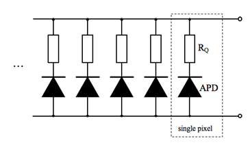
Figure 1. Equivalent circuit of an MPPC. A single pixel is a series combination of an avalanche photodiode and a quenching resistor. All of the pixels are connected in parallel.
In a typical operation, an MPPC is externally reverse-biased with a VBIAS that is up to a few volts greater than the breakdown voltage (VBR) of the APD. An overvoltage, ΔV ≡ VBIAS - VBR, is one of the most important adjustable parameters affecting the performance of the detector, controlling its optical and electrical characteristics such as the gain (M), photon detection efficiency (PDE), and the rates of dark counts, afterpulsing, and optical crosstalk.
In the absence of light and ignoring dark counts, there is no current flowing through a pixel; thus, the voltage on the APD equals VBIAS. That APD is said to be in Geiger mode—a highly unstable state that can be disturbed even by a single photon, leading to the formation of a self-sustained avalanche. The role of RQ in a pixel is to extinguish or quench the avalanche restoring the APD back to Geiger mode. The gain is proportional to the charge released in the avalanche, and its typical values are 105 to 106. Such a high gain is comparable to that of a photomultiplier tube (PMT), making an MPPC its possible substitute in applications involving detection of very faint light. The advantages of an MPPC compared to a PMT are a smaller size, immunity to magnetic fields, and lower biasing voltage. The detector’s disadvantages are that its performance is sensitive to fluctuations of the ambient temperature and of the biasing voltage, the presence of high rates of thermal noise (~ 1 MHz), and of correlated noise: afterpulsing and crosstalk.
Using an MPPC as a light detector in scientific and clinical research requires that the user of the detector understands its optical and electrical behavior under varied environmental conditions, the types and rates of noise, and the limits on reliable light detection. Although manufacturers of MPPCs provide information on their products, an independent check of the detector characteristics, especially in critical situations where a scientific breakthrough hinges on the validity of the observations, is necessary.
This article is a literature survey of experimental techniques used to characterize optical and electrical properties of an MPPC. Section I describes the basic principles behind the operation of first an APD and then an MPPC. Section II presents and discusses experimental setups to measure the most relevant optical and electrical properties of an MPPC. Section III summarizes the main points of the article.
Section I: Background
A light-sensitive APD is a PN junction normally operated in reverse bias close to its VBR. Unlike a photodiode that has a gain M = 1, an APD can have M > 1 owing to multiplication of the photogenerated charge carrier in the avalanche section of the depletion region by impact ionization. The values of M depend on VBIAS with respect to VBR. The following two subsections describe in greater detail the operation of an APD when VBIAS < VBR and VBIAS > VBR, respectively, and an MPPC.
Avalanche photodiode (VBIAS < VBR)
A single pixel in an MPPC is an APD connected in series with a resistor. Figure 2 shows a simplified equivalent circuit of an APD operating at reverse bias that is less than VBR. From left to right, the components are current source, ideal diode, junction capacitance (CJ), junction resistance (RJ), and series resistance (RS).
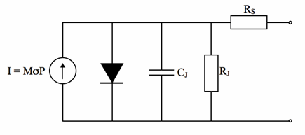
Figure 2. Equivalent circuit of an APD that does not operate in Geiger mode.
The current source outputs current I = MIPH = MσP, where M is the gain and IPH is the photocurrent. The gain is a function of applied voltage, whereas IPH = σP, where σ=σ(λ) is the spectral photosensitivity and P is the power of the incident light. The gain mechanism is avalanche multiplication of charge carriers by impact ionization in the high field region of the APD. If VBIAS < VBR, the avalanche, once triggered, abates completely in finite time.
The behavior of an ideal diode is described by the Shockley equation ID = I0[exp(VD/VT) – 1]. In this equation, ID is the current through the diode, I0 is the reverse saturation current, VD is the voltage on the diode, and VT ≡ kT/e is the thermal voltage, where, k is the Boltzmann constant (k = 8.6 x 10⁻⁵ eV/K), T is temperature, and e is the magnitude of the charge of the electron (e = 1.6×10⁻¹⁹ C). In a typical operation of an APD, VD has a large negative value and, thus, ID ≈ - I0 (the minus sign indicates that this is a reverse current). Note that VD is not an external bias voltage; it is the voltage across the diode and, also, across the current source I, CJ, and RJ.
The capacitor CJ represents the capacitance of the depletion region of the APD. Because the width of the region depends on the voltage across it (which equals VD), CJ = CJ(VD). CJ affects the performance of an MPPC in an important way: it controls the shape of the output current pulse. Therefore, measuring its value as a function of VBIAS constitutes a crucial electrical characterization of the device.
The resistor RJ has a value equal to the resistance of the depletion region. The value depends on the width of the region and on the concentration of charge carriers there. RJ is a complicated function of VD because the latter controls both the width and the degree of impact ionization in the region. When the APD is in Geiger mode and develops an avalanche, RJ becomes negligible.
The resistance RS equals the combined resistance of the undepleted regions in the APD. The value of RS depends on VD since the latter controls the total length of the undepleted regions. RS is on the order of several hundred ohms at zero bias and decreases to tens of ohms around VBR.
Avalanche photodiode (VBIAS > VBR)
When a VBIAS applied to an APD exceeds its VBR, the APD is said to be in Geiger mode. McIntyre (1961) and later Haitz (1964) developed an electrical model (see Figure 3) for an APD operating in this state. Geiger-mode APD is represented by CJ, the switch S, voltage source VBR, and series resistance RS. In the absence of light and ignoring dark events, the switch S is open and CJ is charged to VBIAS. The voltage on the APD is ΔV = VBIAS – VBR above VBR, and the APD is in a highly unstable state. Suppose that the APD absorbs a photon and the resulting charge carrier, either an electron or a hole, triggers an avalanche. At this instant, the switch S closes and CJ begins to discharge through RS, which tends to lower the voltage across the APD. However, since the APD is biased by a constant voltage source VBIAS, current begins to flow through the terminals of the APD reaching a steady state value of ΔV/RS. This current will persist unless VBIAS is reduced to, or below, VBR; doing so restores the APD to the light-sensitive state.
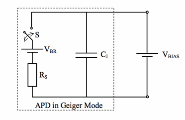
Figure 3. Equivalent circuit of an APD operating in Geiger mode.
Suppose that a resistor RQ >> RS is now connected in series with the Geiger-mode APD, as shown in Figure 4.
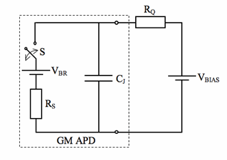
Figure 4. Geiger-mode APD in series with resistor RQ.
In the absence of light and ignoring dark events, the switch S is open and CJ is charged to VBIAS – no current flows through the APD. The APD is in a photosensitive "ready" state. The switch S closes the instant a photogenerated charge carrier triggers an avalanche. CJ begins to discharge through RS; this process tends to lower the voltage across the APD and causes a voltage drop across RQ. The latter implies that a current flows through the terminals of the APD, and Figure 5 depicts its time dependence.
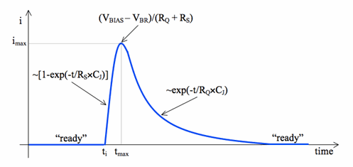
Figure 5. Current flowing through the terminals of the APD as a function of time.
The avalanche begins at t = ti. The leading edge of the current pulse increases with time constant RSCJ and reaches a maximum value of imax = (VBIAS – VBR)/(RQ + RS) ≈ ΔV/RQ at tmax. At around this time the avalanche stops or is quenched because of RQ. After tmax, CJ recharges to the nominal voltage of VBIAS while the current decreases with a time constant RQCJ. Because RQ >> RS the leading edge of the pulse is steeper than the trailing (or declining) edge; the pulse is asymmetric around t = tmax. For a more detailed discussion of the electrical behavior of Geiger-mode APD see Haitz (1964).
MPPCs are designed so that imax (referred to as the "latch" current) is about 20 μA. The condition for proper quenching is 0 < ΔV < RQimax. For ΔV = 1 V, the minimum RQ is 50 kΩ. If RQ is set below this limit, the quenching time increases, which would show as flattening of the current pulse around tmax. If RQ is substantially below the minimum limit, the quenching never occurs and the current becomes constant with an amplitude of (VBIAS – VBR)/(RQ + RS).
Integrating the current pulse with respect to time yields the total charge Q that transferred between the terminals of the APD. Since the transfer was triggered by a single charge carrier, the gain M = Q/e. A detailed analysis shows that Q = CJΔV and, thus, M = CJΔV/e.
MPPC
The MPPC is a rectangular array of light-sensitive elements—pixels—that are all connected in parallel and externally biased by a single voltage source, VBIAS. Each pixel is a series combination of an APD and a resistor RQ. By design, all pixels are identical. The pixels operate in Geiger mode, that is, VBIAS > VBR, or ΔV > 0.
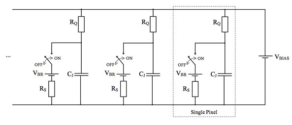
Figure 6. Equivalent circuit of an MPPC.
Figure 6 shows an equivalent circuit of an MPPC; the dotted rectangle delineates a single pixel. In the absence of light and ignoring dark counts, all of the switches are in the OFF position, and the voltage is VBIAS on each APD and is zero on each RQ. Suppose that a single APD absorbs a photon and the process triggers an avalanche. At this instant, the switch in the equivalent circuit of that APD goes to the ON position, and the current pulse begins to flow through the terminals of the MPPC as shown in Figure 5. RQ of that pixel quenches the avalanche, and the pixel is restored back to the "ready" state. If two (or more) photons simultaneously trigger avalanches in two (or more) distinct pixels, the current pulse flowing through the terminals of the MPPC is a superposition of the current pulses generated by the two (or more) pixels. In contrast, if a single pixel absorbs simultaneously two or more photons, the ensuing current pulse is identical to the one produced by a single photon.
When a pixel recovers from the avalanche, its CJ recharges to the nominal voltage VBIAS. At the outset of the recharge process, the current flows from VBIAS but also from the junction capacitors of all other pixels. The latter current keeps lowering ΔV on the other pixels until the value equals the ΔV on the recovering pixel. At this instant, VBIAS becomes the only source of current, and all of the pixels recharge together back to VBIAS.
Section II: Characterization of an MPPC
This section describes experimental methods of measuring electrical and optical characteristics of an MPPC.
Measuring RQ and CJ
The forward-bias I-V characteristic of an MPPC (e.g., see Figure 10) can be used to measure the approximate value of RQ. The I-V characteristic can be obtained with a circuit shown in Figure 7. Assuming that RQ is the same for each pixel and that RQ >> RS, the slope of the linear region in the first quadrant equals N/RQ, where N is the number of pixels. Thus, RQ = N/slope.
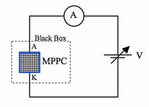
Figure 7. The electrical circuit to obtain a forward-bias I-V characteristic, which contains information about RQ. The MPPC must be shielded from light in a temperature-controlled environment.
Figure 8 shows an equivalent circuit of an MPPC that illustrates how CJ of a single pixel can be measured. There are N pixels connected in parallel, where one pixel is represented by CJ in parallel with RJ and this combination is in series with RS + RQ. The terminals of the MPPC are at the right.
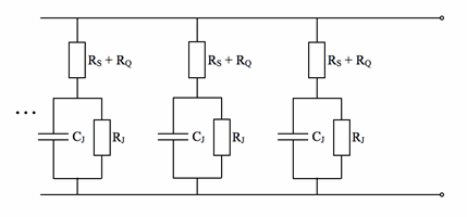
Figure 8. Equivalent circuit of an MPPC to illustrate how to measure CJ.
The impedance Z of the network as seen from the terminals of the MPPC is given by the following equation.
Equation 1: Impedance of the MPPC shown in Figure 8.
Equation 1 implies that the effective capacitance seen at the terminals of the MPPC is NCJ, the capacitance of a single pixel multiplied by the number of pixels. Because CJ is a function of reverse voltage, the Keithley C-V 590 analyzer is well-suited for determining this dependence. Figure 9 shows the block diagram of the experimental setup.
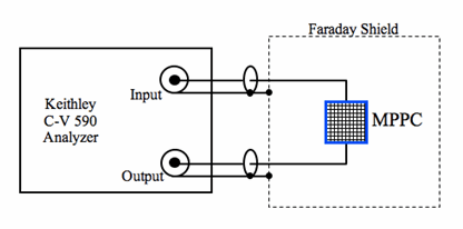
Figure 9. Connection schematic to measure junction capacitance of an MPPC as a function of reverse voltage.
The MPPC is inside a temperature-controlled lightproof Faraday shield. The terminals of the detector are connected to the input and output of the C-V 590 using BNC cables. The "ground" of the cables is connected to the shield. The polarity of the connection is such that when the C-V 590 performs the voltage sweep, the MPPC is reverse-biased.
Figure 10 is an example of forward and reverse I-V and C-V characteristics for an MPPC with 667 pixels. The forward I-V characteristic becomes linear at a bias voltage of around 0.7 V. The inverse of the slope in the linear region is about 225 Ω implying that RQ ≈ 150 kΩ. The reverse-bias I-V characteristic shows that the breakdown voltage VBR ≈ 70 V (reverse).
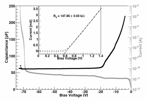
Figure 10. Forward and reverse I-V characteristics and C-V characteristic of an MPPC. Adapted from Vacheret et al. (2011).
The combined junction capacitance N x CJ decreases steeply when the reverse voltage increases from 5 V to 20 V. Above 20 V, the decrease is much less pronounced; at around VBR, N x CJ ≈ 60 pF, or CJ ≈ 90 fF.
Observing noise
An MPPC generates three noise components: dark noise (or dark counts), afterpulses, and optical crosstalk. Thermally generated charge carriers that trigger an avalanche are responsible for dark noise. Dark noise is random and is always present regardless of the light level illuminating the MPPC. Its rate (number of pulses per unit time) increases with temperature and ΔV. The presence of the other two noises is correlated to the occurrence of an avalanche, which has been triggered either by a photogenerated or thermally generated (dark) charge carrier. A release of a trapped charge in a pixel experiencing an avalanche can trigger a secondary avalanche while the pixel is recovering from the primary avalanche. This is afterpulsing. Optical crosstalk arises when an avalanche in a pixel emits photons that trigger one or more avalanches in the adjoining pixels. The resulting output signal is a superposition of the signals from the "fired" pixels.
Figure 11 illustrates an experimental setup to observe and record the three noise components. An MPPC is inside a temperature-controlled dark box. The variable high voltage source (e.g., Keithley 487) reverse-biases the MPPC and sets the value of ΔV. The output signal from the MPPC is AC-coupled to a "fast" amplifier (e.g., Hamamatsu C5594) using a 10 kΩ load resistor and 100 nF coupling capacitor. The output of the amplifier connects to a digital oscilloscope (e.g., LeCroy Wave Pro 7300A). The values of the load resistor and the coupling capacitor can be adjusted to optimize the fidelity of the displayed signals.
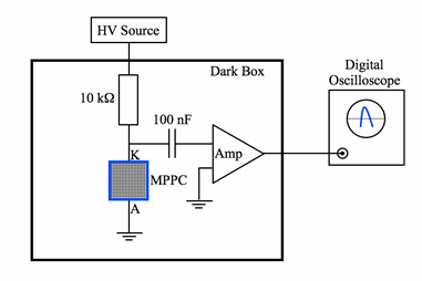
Figure 11. Experimental setup to observe the noise components in an MPPC.
Figure 12 is an example of an oscilloscope display showing an accumulation of waveforms (the persistence was set to 10 s) resulting from the three types of noise. The most numerous waveforms are due to random dark noise. Such a waveform is indistinguishable from the one that would have been produced had the avalanche been triggered by a photogenerated charge carrier. A waveform due to afterpulsing trails (in time) the primary waveform—a waveform due to dark noise. The delay is on the order of tens of ns. The signals due to optical crosstalk are practically in phase with the primary signal and, thus, the resulting waveform is the superposition of the signals. Those that are labeled 2 p.e. (3 p.e.) result when one (two) neighboring pixel is (are) affected.
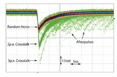
Figure 12. Oscilloscope display (10 s persistence) showing waveforms corresponding to random dark noise, correlated noise due to afterpulsing, and correlated noise due to optical crosstalk. Adapted from Murase et al. (2009).
Measuring crosstalk
In the absence of light, 2 p.e. (or greater) waveforms originating from an MPPC can be either due to random dark noise occurring in two or more pixels simultaneously or crosstalk. The probability of the former is very small and will be neglected. Therefore, counting the number of waveforms above the 1 p.e. threshold per unit time yields the crosstalk rate, while dividing this rate by the rate of 1 p.e. waveforms yields the crosstalk probability.
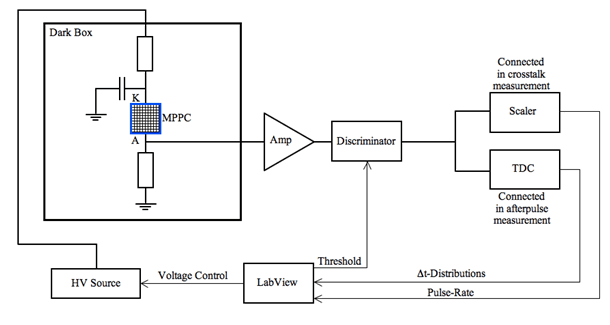
Figure 13. Experimental setup to measure the rates of crosstalk and afterpulsing. Adapted from Eckert et al. (2010).
Figure 13 is an experimental setup to measure the rates (and probabilities) of crosstalk and afterpulsing. The MPPC is inside a temperature-controlled and light-leak-proof dark box reverse-biased by a high voltage source. The amplifier amplifies the output signal from the MPPC and feeds the resulting signal to the discriminator. If the input crosses a user-specified threshold level, the discriminator issues a logical output pulse of some duration (several ns), which the Scaler module, with its gate set to 1 s, counts. Figure 14 shows an example of a resulting count rate as a function of the threshold level for the Hamamatsu S10362-11-050C MPPC operating at ΔV = 1.3 V.
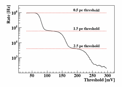
Figure 14. Noise rate as a function of the discriminator threshold for the Hamamatsu S10362-11-050C MPPC operating at ΔV = 1.3 V. Adapted from Eckert et al. (2010).
Figure 14 shows that the noise rate, ν, decreases with the discriminator threshold level showing a characteristic step-like dependence. The horizontal red dashed lines delineate the values of ν for the threshold levels that correspond to 0.5 p.e., 1.5 p.e., and 2.5 p.e., respectively. Setting the threshold level to 0.5 p.e., which is above the electronic noise but below 1 p.e., gives the rate of the total dark noise ν0.5 p.e.. Setting the threshold to 1.5 p.e. gives the rate of the events due to crosstalk ν1.5 p.e.. The probability of crosstalk PC is therefore given by PC = ν0.5 p.e./ ν1.5 p.e..
The crosstalk probability PC depends on the overvoltage ΔV, and the experimental setup depicted in Figure 13 can also be used to determine this dependence. The procedure is to measure PC as outlined above for different values of ΔV, which is controlled by the high voltage source. Figure 15 is an example of the resulting dependence (note that the gain and ΔV are linearly proportional to each other). The figure shows that PC steeply increases with ΔV for all of the tested MPPCs.
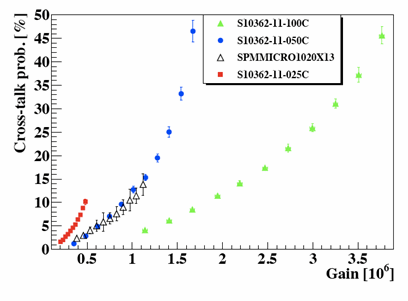
Figure 15. Crosstalk probability as a function of gain (proportional to ΔV). Adapted from Eckert et al. (2010).
Measuring afterpulsing
When a pixel develops an avalanche, some charge carriers can be trapped by lattice defects. Their subsequent release, while the pixel recovers from the primary avalanche, can trigger a secondary correlated avalanche—an afterpulse. The amount of charge released in an afterpulse depends on the time delay Δt between the primary and secondary avalanches, or the recovery state of the pixel. The ratio of charge released in an afterpulse and that released in the primary avalanche can be modeled by the following equation.
Equation 2: Charge ratio.
In this equation, τr is the recovery time (from an avalanche) of a pixel. If Δt is small compared to τr, then ξ is small implying that an afterpulse has amplitude less than 1 p.e. The amplitude of an afterpulse increases as Δt increases and in the limit Δt >> τr it is 1 p.e. In this limit, the afterpulse is indistinguishable from a signal that was generated either thermally or optically.
An experimental setup depicted in Figure 13 can be used to measure the probability of afterpulsing Pap. Here, the Scaler is replaced with Time-to-Digital Converter (TDC), which measures Δt for consecutive pulses coming from the discriminator (threshold level at 0.5 p.e.). The solid black curve in Figure 16 is an example of the measured dark noise time-difference distribution. For Δt < 20 ns, the distribution is unreliable because to detect an afterpulse, the primary signal must fall below the discriminator threshold level; the time to do so is on the order of 10 – 15 ns (see Figure 12). For Δt greater than the pixel recovery time, the dark-noise time-difference distribution can be modeled as the sum of two probability density functions [what follows is from Eckert et al. (2010)].
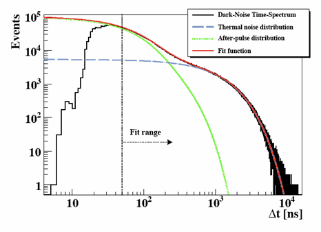
Figure 16. Dark noise time-difference distribution (black solid curve) for Hamamatsu S10362-11-050C at a reverse bias of 70.6 V. Adapted from Eckert et al. (2010).
Equation 3 is a model probability density function for events due to thermal pulses. Here, Ntp is the integrated number of thermal events and 1/τtp is the rate (or frequency) of these events.
Equation 3: Probability density function for events due to thermal pulses.
Equation 4 is a model probability distribution function for events due to afterpulsing. The function is a sum of two exponentials: the first exponential term models "fast" events with a characteristic time τapf, whereas the second models "slow" events with a characteristic time τaps. The parameters Napf and Naps are the integrated number of "fast" and "slow" events, respectively.
Equation 4: Probability density function for events due to afterpulses.
The probability density functions given by Equation 3 and Equation 4 are simultaneously fitted to the data, as shown in Figure 16. The fit yields the values of the adjustable parameters in the probability density functions.
With the adjustable parameters determined from the fit, Equation 5 can be used to calculate the probability of afterpulsing. Equation 2 gives the charge ratio function ξ. To evaluate the integral it is necessary to adopt the appropriate pixel recovery time τr.
Equation 5: Probability of afterpulses.
The probability of afterpulses Pap is a function of overvoltage ΔV for two reasons. As ΔV increases: (1) the amount of charge in a primary avalanche increases making charge trapping more likely and (2) the probability that a charge carrier triggers an avalanche in the depletion region increases. The same experimental setup and analysis as described above can be used to determine how Pap depends on ΔV by varying the bias voltage on the MPPC. Figure 17 is an example of such dependence for three MPPCs manufactured by Hamamatsu.
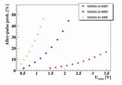
Figure 17. Probability of afterpulsing as a function of overvoltage. Adapted from Eckert et al. (2010).
Measuring photon detection efficiency
The photon detection efficiency, PDE, of an MPPC is defined as the product of quantum efficiency η, the geometrical fill factor Fg, and a combined probability Pa of electrons and holes initiating Geiger-mode avalanche; that is, PDE = ηFgPa. The value of η is a probability that a photon generates a charge carrier that enters the avalanche region in a pixel. It is a function of the wavelength of light λ and temperature T, but it is independent of ΔV for full depletion. The geometrical fill factor Fg is a ratio of the combined photosensitive area to the total area of an MPPC. Due to edge effects, Fg exhibits a weak dependence on ΔV. The avalanche probability Pa is a function of λ, T, and ΔV.
The PDE is a crucial parameter in photon counting experiments; therefore, its value must be known for a given wavelength and overvoltage if absolute photon fluxes are to be measured.
PDE versus overvoltage
Figure 18 shows an experimental setup to measure the PDE of an MPPC as a function of ΔV using a pulsed-LED method discussed in Musienko et al. (2006) and Vacheret et al. (2011).
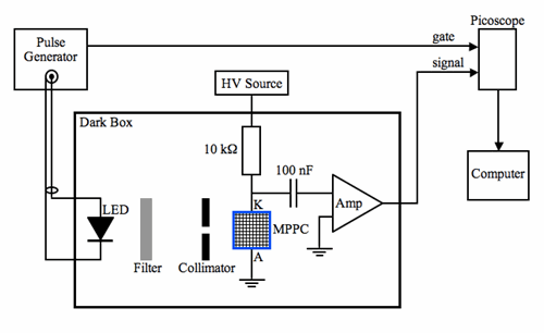
Figure 18. Experimental setup to measure PDE as a function of overvoltage.
An LED with a narrow emission spectrum emits pulses of light with a duration and repetition rate set by the pulse generator. The neutral density filter controls the number of photons per pulse, and the collimator allows a uniform illumination of the photosensitive section of an MPPC. The optical depth of the filter is adjusted so that 2 to 5 pixels are activated per pulse. The number of photons per pulse Nγ arriving at the plane of the MPPC must be measured using a calibrated photodetector, such as the XP2020 or R7899 PMTs. The high-voltage source, such as the Keithley 487, reverse-biases an MPPC and determines the value of ΔV. A fast transimpedance amplifier amplifies the output signal, and the picoscope, such as the PicoScope 5023, digitizes and integrates the output to obtain a charge amplitude spectrum such as the one shown in Figure 19.
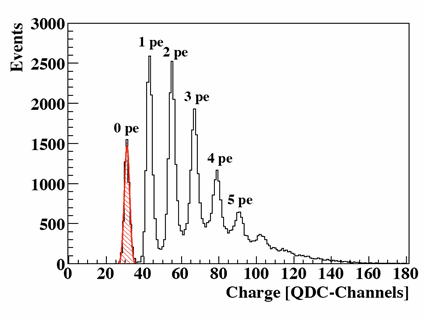
Figure 19. Example of single photon charge spectrum. A peak in the spectrum corresponds to a certain number of photoelectrons, e.g., 0 pe, 1 pe, etc. Adapted from Eckert et al. (2010).
The probability P of detecting n photons by an MPPC is given by the Poisson distribution.
Equation 6: The probability of detecting n photons by an MPPC is given by Poisson distribution.
In this equation, npe is the average number of photoelectrons. The events for n = 0 (no photon detected) correspond to the "pedestal" on the charge amplitude spectrum; the subsequent peaks are for n =1, 2, … (see Figure 19). The values of P(n, npe) for n > 0 are distorted by the presence of crosstalk and afterpulsing, but the value for n = 0 is not. Measuring P(0, nnp), which is the ratio of the number of events in the pedestal N0 and the total number of events NT, allows unbiased determination of npe. Both N0 and NT are determined from the charge amplitude spectrum. Since P(0, npe) = N0/NT = exp(-npe), then npe = -ln(N0/NT). Taking into account dark pulses, npe is given by the following.
Equation 7: Average number of photoelectrons.
Here, N0D and NTD are the number of events in the pedestal and the total number of events, respectively, in a charge amplitude spectrum taken under dark conditions (see Figure 20). Thus, the PDE is given by Equation 8.
Equation 8: The PDE is a ratio of the average number of photoelectrons and the average number of photons per pulse.
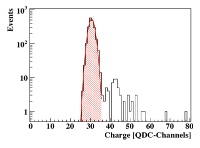
Figure 20. Thermal noise charge spectrum taken under dark conditions. Adapted from Eckert et al. (2010).
Measuring gain and breakdown voltage
A charge amplitude spectrum of an MPPC, such as the one depicted in Figure 19, can be used to determine the gain M of the device using the following equation.
Equation 9: Gain of an MPPC using information from charge amplitude spectrum.
In the equation, QDCcal is the charge per one channel of QDC (charge-to-digital converter), Δpp is the number of channels separating two adjacent peaks, Kamp is the amplification factor of the electronics, and e is the value of the fundamental charge. If charge amplitude spectra are collected for various settings of VBIAS, M as a function of VBIAS can be determined, as shown in Figure 21.
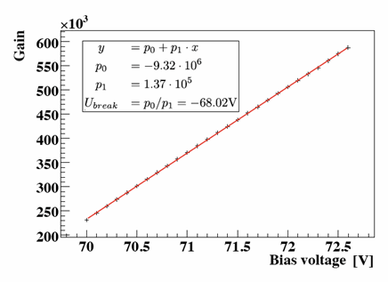
Figure 21. Gain versus bias voltage. Adapted from Eckert et al. (2010).
As expected, the relationship between M and VBIAS is linear with the slope and vertical-intercept equal to CJ/e and CJVBR/e, respectively. Fitting a straight line to the data yields the values of CJ and VBR.
Measuring time jitter
Suppose that a photodetector is illuminated with δ-function pulses of light that are equally spaced in time with period T and, in response, the detector produces output signal pulses. If the time interval between the consecutive output pulses varies, the output does not have the same period T and the detector is said to exhibit "time jitter."
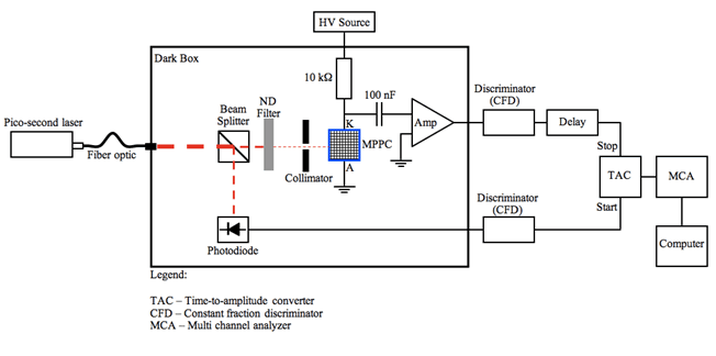
Figure 22. A possible experimental setup to measure the time jitter of an MPPC used by Nagano et al. (2012).
Figure 22 shows a possible experimental setup (Nagano et al. 2012) to measure the time jitter of an MPPC. The detector is inside a temperature-controlled dark box. A picosecond laser (λ = 650 nm, 70 ps pulse width, 1 kHz repetition rate, and time jitter less than 10 ps) is the source of light. The beam splitter divides the beam into two beams. One illuminates a photodiode and the other—after passing through a neutral density filter and collimator—the MPPC. The filter and collimator combination can be adjusted to vary the number of photons per pulse striking the MPPC. The output from the photodiode, after passing through a constant fraction discriminator (CFD), provides the "start" pulse to the time-to-amplitude (TAC) converter. The role of the CFD is to filter out noise: only those signals for which the value of the leading edge exceeds some fraction (e.g., 30%) of the difference between the peak value and the base level are permitted. After being amplified by a factor of 30 to 50, the output from the MPPC passes through the CFD and delay circuit (or line) and arrives at the TAC providing the "stop" pulse. The TAC outputs a signal whose amplitude is proportional to the time difference between the start and stop pulses. The multi-channel analyzer (MCA) stores and sorts the pulses according to their height, and displays their histogram, or spectrum, such as that displayed in Figure 23.
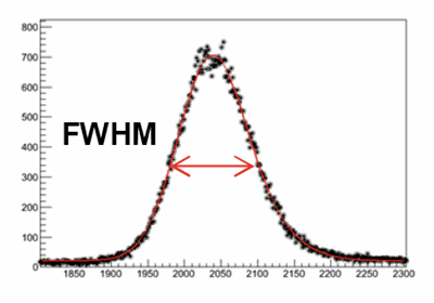
Figure 23. Histogram produced by MCA. The horizontal axis is proportional to the time difference between the "start" and "stop" pulses arriving at the TAC. Adapted from Nagano et al. (2012).
For a normal distribution, the full-width at half maximum (FWHM) is a measure of the total time jitter: FWHM = 2.355σT. If the time jitters of the individual components of the setup are independent of one another, the sum of their squares equals σT2. From the time jitters of the laser pulses, photodiode, and the combined electronics, the time jitter of the MPPC can be calculated.
Measuring linearity and dynamic range
An MPPC consists of N pixels where each pixel can exist in only two states: ON or OFF. A pixel in the OFF state switches to the ON state if it absorbs one or more photons and the resulting photogenerated charge carriers trigger an avalanche. The maximum possible output signal from an MPPC is N p.e. in response to a δ-pulse of light containing Nγ photons. Thus, the total number of pixels determines the dynamic range of the detector.
Equation 10 is a model that gives the number of pixels that have turned ON (or that have "fired") in response to Nγ of incident photons on the surface of an MPPC with N pixels and the photon detection efficiency PDE.
Equation 10: Number of pixels Nf that have turned ON ("fired") in response to Nγ of incident photons on an MPPC with N pixels and the photon detection efficiency PDE.
If the product of Nγ and PDE is much smaller than N, Equation 10 reduces to Nf = NγPDE. Here, the response of the detector is linear with PDE being the constant of proportionality between Nf and Nγ. However, in the limit NγPDE → ∞, Nf → N, the saturation limit.
Gruber et al. (2014) have investigated how a variety of MPPCs respond to pulses of light (32 ps FWHM duration and λ = 404 nm) containing from one to thousands of photons using a setup depicted in Figure 24. The PIN photodiode can be calibrated at low light levels (where NγPDE << N) so that its output is proportional to Nseed ≡ NγPDE at any light level. Here, Nseed is the average number of photons incident on the photosensitive area of an MPPC. Thus, the output from the PIN photodiode yields Nseed and the scope yields the height of the output signal, which is proportional to Nf. The setup, thus, allows a measurement of Nf as a function of Nseed for different settings of overvoltage and of different MPPCs. The results can be normalized to allow a direct comparison among the MPPCs used in the tests and comparison to the predictions from Equation 10.
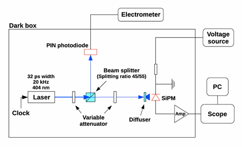
Figure 24. Experimental setup to investigate linearity and saturation limit of MPPCs. Adapted from Gruber et al. (2014).
The results are surprising. Figure 25 shows the response curves of four different MPPCs normalized to the total number of pixels in each MPPC for high light levels (left panel) and medium to low light levels (right panel). The figure shows that the outputs from the MPPCs are fairly linear and consistent with Equation 10 up to Nseed/N ≈ 0.5. Above this limit, the outputs are larger than the predictions from Equation 10 (Equation 3 in the original study) and the saturation level may be more than 2N (Hamamatsu 050U MPPC), in disagreement with Equation 10. The study finds no acceptable explanation for this "oversaturation" and questions our current understanding of how the device operates.
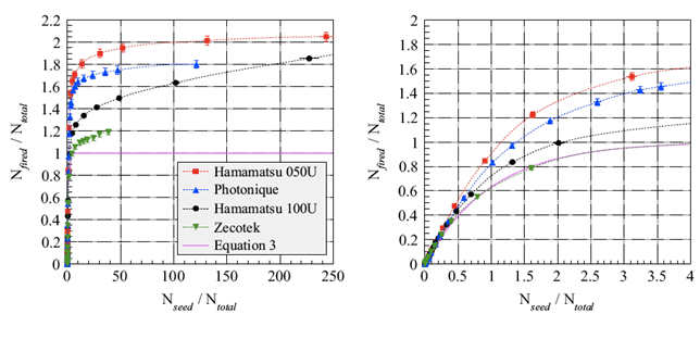
Figure 25. Response curves of four MPPCs for high light levels (left panel) and medium to low light levels (right panel). Adapted from Gruber et al. (2014).
Section III: Summary
This article is a review of the experimental methods to characterize optical and electrical properties of an MPPC. The following are the main points of the article:
- An MPPC is an array of pixels connected in parallel where one pixel is a series combination of an APD and a quenching resistor. The APD is externally biased to operate in Geiger mode.
- The junction capacitance and quenching resistance are key electrical parameters of an MPPC. Both can be measured from forward and reverse I-V characteristics of the device.
- Three major sources of noise exist in an MPPC: thermally induced random dark counts, correlated optical crosstalk, and afterpulsing. The rates of these noises as a function of temperature and overvoltage can be measured, and these rates will enter into the calculations of the photon flux on the detector.
- Photon detection efficiency is a ratio of the detected number of photoelectrons to the number of photons in a pulse of light. Knowing how this parameter depends on the wavelength of light and overvoltage is crucial in all photon counting experiments. This article describes a method of measuring this parameter, correcting for the presence of noise.
- The time interval between the instant when a photon strikes a pixel of an MPPC and the instant the device produces an output varies in a sequence of events. The rms of the variation is known as time jitter—a crucial characteristic in experiments involving time-of-flight or coincidence. Time jitter is a function of the wavelength of light, overvoltage, and temperature. This article describes a method of measuring this parameter.
- The total number of pixels of an MPPC limits its dynamic range.
- The output of an MPPC is linear in a regime where the product of the number of the incident photons and the photon detection efficiency is much smaller than the total number of pixels. MPPCs exhibit a phenomenon of "oversaturation" where the output signal may exceed N p.e. (N is the number of pixels) in response to a pulse of light containing Nγ of photons. This phenomenon is not well understood.
References
- P. Eckert, H.C. Schultz-Coulon, W. Shen, R. Stamen and A. Tadday, "Characterization studies of silicon photomultipliers," Nucl. Instrum. and Meth. A 620 (2010): 217-26.
- R. H. Haitz, "Model for the Electrical Behavior of a Microplasma," J. of Appl. Phys., vol. 35, no. 2 (1964): 1370-1376.
- L. Gruber, S. E. Brunner, J. Marton, K. Suzuki, "Over saturation behavior of SiPMs at high exposure," Nucl. Instrum. Meth. A 737 (2014): 11-18.
- R. J. McIntyre, "Theory of Microplasma Instability in Silicon," J. of Appl. Phys., vol. 32, no. 6 (1961): 983-995.
- T. Murase, H. Oide, H. Otono, S. Yamashita, "Development of PPD: characterization and simulation," International Workshop on New Photon Detectors PD09, June 24-26 2009, Shinshu University, Matsumoto, Japan.
- Y. Musienko, S. Reucroft and J. Swain, "The gain, photon detection efficiency and excess noise factor of multi-pixel Geiger-mode avalanche photodiodes," Nucl. Instrum. Meth. A 567 (2006): 57.
- T. Nagano, K. Sato, A. Ishida, T. Baba, R. Tsuchiya, K. Yamamoto, "Timing Resolution Improvement of MPPC for TOF-PET Imaging," 2012 IEEE Nuclear Science Symposium and Medical Imaging Conference Record (NSS/MIC).
- A. Vacheret, G. J. Barker, M. Dziewiecki, P. Guzowski, M. D. Haigh, B. Hartfiel, A. Izmaylov, W. Johnston, M. Khabibullin, A. Khotjantsev, Y. Kudenko, R. Kurjata, T. Kutter, T. Lindner, P. Masliah, J. Marzec, O. Mineev, Y. Musienko, S. Oser, F. Retiere, R. O. Salih, A. Shaikhiev, L. F. Thompson, M. A. Ward, R. J. Wilson, N. Yershov, K. Zaremba and M. Ziembicki, "Characterization and simulation of the response of multi-pixel photon counters to low light levels," Nucl. Instrum. Methods Phys. Res. A vol. 656, no. 1 (2011): 69-83.
- Confirmation
-
It looks like you're in the . If this is not your location, please select the correct region or country below.
You're headed to Hamamatsu Photonics website for US (English). If you want to view an other country's site, the optimized information will be provided by selecting options below.
In order to use this website comfortably, we use cookies. For cookie details please see our cookie policy.
- Cookie Policy
-
This website or its third-party tools use cookies, which are necessary to its functioning and required to achieve the purposes illustrated in this cookie policy. By closing the cookie warning banner, scrolling the page, clicking a link or continuing to browse otherwise, you agree to the use of cookies.
Hamamatsu uses cookies in order to enhance your experience on our website and ensure that our website functions.
You can visit this page at any time to learn more about cookies, get the most up to date information on how we use cookies and manage your cookie settings. We will not use cookies for any purpose other than the ones stated, but please note that we reserve the right to update our cookies.
1. What are cookies?
For modern websites to work according to visitor’s expectations, they need to collect certain basic information about visitors. To do this, a site will create small text files which are placed on visitor’s devices (computer or mobile) - these files are known as cookies when you access a website. Cookies are used in order to make websites function and work efficiently. Cookies are uniquely assigned to each visitor and can only be read by a web server in the domain that issued the cookie to the visitor. Cookies cannot be used to run programs or deliver viruses to a visitor’s device.
Cookies do various jobs which make the visitor’s experience of the internet much smoother and more interactive. For instance, cookies are used to remember the visitor’s preferences on sites they visit often, to remember language preference and to help navigate between pages more efficiently. Much, though not all, of the data collected is anonymous, though some of it is designed to detect browsing patterns and approximate geographical location to improve the visitor experience.
Certain type of cookies may require the data subject’s consent before storing them on the computer.
2. What are the different types of cookies?
This website uses two types of cookies:
- First party cookies. For our website, the first party cookies are controlled and maintained by Hamamatsu. No other parties have access to these cookies.
- Third party cookies. These cookies are implemented by organizations outside Hamamatsu. We do not have access to the data in these cookies, but we use these cookies to improve the overall website experience.
3. How do we use cookies?
This website uses cookies for following purposes:
- Certain cookies are necessary for our website to function. These are strictly necessary cookies and are required to enable website access, support navigation or provide relevant content. These cookies direct you to the correct region or country, and support security and ecommerce. Strictly necessary cookies also enforce your privacy preferences. Without these strictly necessary cookies, much of our website will not function.
- Analytics cookies are used to track website usage. This data enables us to improve our website usability, performance and website administration. In our analytics cookies, we do not store any personal identifying information.
- Functionality cookies. These are used to recognize you when you return to our website. This enables us to personalize our content for you, greet you by name and remember your preferences (for example, your choice of language or region).
- These cookies record your visit to our website, the pages you have visited and the links you have followed. We will use this information to make our website and the advertising displayed on it more relevant to your interests. We may also share this information with third parties for this purpose.
Cookies help us help you. Through the use of cookies, we learn what is important to our visitors and we develop and enhance website content and functionality to support your experience. Much of our website can be accessed if cookies are disabled, however certain website functions may not work. And, we believe your current and future visits will be enhanced if cookies are enabled.
4. Which cookies do we use?
There are two ways to manage cookie preferences.
- You can set your cookie preferences on your device or in your browser.
- You can set your cookie preferences at the website level.
If you don’t want to receive cookies, you can modify your browser so that it notifies you when cookies are sent to it or you can refuse cookies altogether. You can also delete cookies that have already been set.
If you wish to restrict or block web browser cookies which are set on your device then you can do this through your browser settings; the Help function within your browser should tell you how. Alternatively, you may wish to visit www.aboutcookies.org, which contains comprehensive information on how to do this on a wide variety of desktop browsers.
5. What are Internet tags and how do we use them with cookies?
Occasionally, we may use internet tags (also known as action tags, single-pixel GIFs, clear GIFs, invisible GIFs and 1-by-1 GIFs) at this site and may deploy these tags/cookies through a third-party advertising partner or a web analytical service partner which may be located and store the respective information (including your IP-address) in a foreign country. These tags/cookies are placed on both online advertisements that bring users to this site and on different pages of this site. We use this technology to measure the visitors' responses to our sites and the effectiveness of our advertising campaigns (including how many times a page is opened and which information is consulted) as well as to evaluate your use of this website. The third-party partner or the web analytical service partner may be able to collect data about visitors to our and other sites because of these internet tags/cookies, may compose reports regarding the website’s activity for us and may provide further services which are related to the use of the website and the internet. They may provide such information to other parties if there is a legal requirement that they do so, or if they hire the other parties to process information on their behalf.
If you would like more information about web tags and cookies associated with on-line advertising or to opt-out of third-party collection of this information, please visit the Network Advertising Initiative website http://www.networkadvertising.org.
6. Analytics and Advertisement Cookies
We use third-party cookies (such as Google Analytics) to track visitors on our website, to get reports about how visitors use the website and to inform, optimize and serve ads based on someone's past visits to our website.
You may opt-out of Google Analytics cookies by the websites provided by Google:
https://tools.google.com/dlpage/gaoptout?hl=en
As provided in this Privacy Policy (Article 5), you can learn more about opt-out cookies by the website provided by Network Advertising Initiative:
http://www.networkadvertising.org
We inform you that in such case you will not be able to wholly use all functions of our website.
Close