Application notes

Technical notes
Ask an engineer


Publications
United States (EN)
Select your region or country.
A technical guide to silicon photomultipliers (MPPC) - Section 1
Ardavan Ghassemi, Hamamatsu Corporation
Kota Kobayashi & Kenichi Sato, Hamamatsu Photonics K.K.
January 11, 2018
1. Operation principles & characteristics
Technological evolution from Si PN/PIN photodiodes to APD and MPPC
1-1. The PN junction & unity-gain Si photodiodes
Silicon PN and PIN photodiodes are the most basic of silicon photodetectors; a fundamental understanding of their operation principles is essential for our discussion.
Crystalline silicon at highest levels of purity has a steady equilibrium of negative (electrons) and positive (holes) charge carriers; despite possible local fluctuations, neither carrier type can attain general majority. This state of silicon crystal is referred to as intrinsic as almost no foreign impurities are present within the crystal lattice; intrinsic silicon’s resistance is quite high, making it unsuitable for efficient charge collection. Si PN photodiodes are fabricated by forming a PN junction in crystalline silicon by doping1 a portion of it with electron donors (i.e. atoms of group V elements like phosphorus or arsenic with five electrons in their outermost electron orbital) to form an N region (where negatively-charged electrons become the majority charge carrier) and by doping an adjacent portion with electron acceptors (i.e. atoms of group III elements like boron or aluminum with one electron in their outermost orbital) to form a neighboring P region (where positively-charged holes become the majority charge carrier). Since each silicon atom has four electrons in its outermost orbital, a donor atom can share four of its outermost electrons with neighboring silicon atoms to form an electrovalent bond with them and participate in the silicon lattice structure by donating its fifth outermost electron to the conduction band (a lattice-wide energy level in which an electron can move from an atom to another within the crystal lattice) at room temperature. Likewise, an acceptor atom can share its three outermost electrons with neighboring Si atoms and join the crystal lattice by accepting an electron and thus introducing a hole (i.e. an absence of electron) into the valence band (a lattice-wide energy level in which a hole can move from an atom to another within the crystal lattice) at room temperature.
1 Doping is a phenomenon that can be appropriately described as forming a solid-state solution through Brownian motion of the dissolved impurity atoms (i.e. dopants) into silicon (as the solvent) at elevated temperatures, which results in the dopant atoms participating in the silicon crystal lattice structure. To create this solution, the impurity atoms must be introduced into the silicon bulk by either of two means: i. Diffusion in which the Brownian motion begins by deposition of the dopant atoms at the silicon surface and progresses in depth away from the silicon surface into the silicon bulk (as a spreading Gaussian profile) by thermal agitation, and ii. Ion implantation in which the silicon bulk is bombarded by high-energy ions using an industrial particle accelerator or RF plasma oscillator; this bombardment is then followed by a phase of thermal annealing that allows the bombardment damage to the silicon lattice to be repaired while (in a similar manner to diffusion) the dopant atoms are spread away from their peak concentration (at the mean bombardment depth) by the Gaussian profile of Brownian motion and concurrently get positioned within the lattice structure. Generally speaking, diffusion is suitable for forming large but coarse doped regions at shallow depths while ion implantation is used for creating deep-buried junctions of fine size or precise profile.
The resulting P (anode) and N (cathode) regions are commonly referred to as extrinsic with much lower resistance than intrinsic silicon as increases in majority carrier concentration decrease electrical resistance of a doped region. Since all participating atoms in the lattice of a monolithic semiconductor crystal share the same valence and conduction band energy levels, electrons in the conduction band and holes in the valence band can roam within the crystal’s physical dimensions. Either carrier type can, however, enjoy far greater mobility under an electric field by drifting rapidly across the E-field than to diffuse through the semiconductor crystal by Brownian random walk in the absence of an electric field.
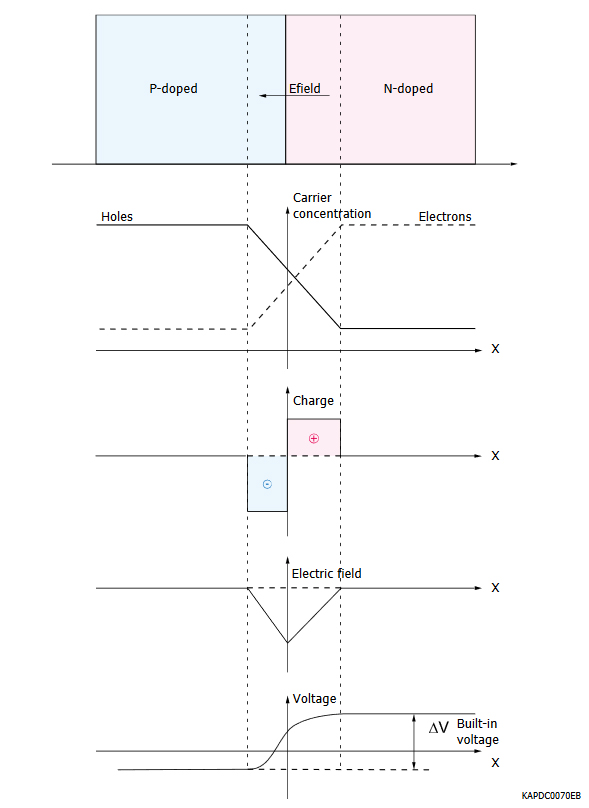
Figure 1-1 The PN junction under equilibrium
Once a PN junction is formed, considering that its N and P regions have a large concentration gradient of majority carriers between them, a diffusion current appears with electrons diffusing from the N side and holes diffusing from the P side towards the opposite side in order to recombine (i.e. a hole and an electron recombine to neutralize each other’s electrical charge). The resulting recombination process depletes the layer adjacent to the junction on each side from majority carriers (hence forming what is called the depletion layer). Since there is an immobile ionized donor or acceptor atom in the lattice for every majority carrier (conduction electron or valence hole) in a doped region, opposite charges form in the depletion layer from acceptor and donor ions whose hole and electron contributions have recombined and been neutralized. Consequently, the depletion layer’s N-region side (with an electron majority) becomes positive due to loss of its electrons (and because of its uncompensated donor ions); the depletion layer’s P-region side (with a hole majority) becomes negative due to loss of its holes (and because of its uncompensated acceptor ions). These charges cause the formation of an electric field across the depletion layer that points from the layer’s positively-charged N side towards its negatively-charged P side. Pointing from the cathode (i.e. the N region) to the anode (i.e. the P region), this electric field is considered to have a negative polarity by convention; it has an absolute intensity peaking at the PN junction (where distance between opposing charges is minimal) and rolling off farther away from it into each side of the depletion layer.
While being formed, this electric field exerts a force on diffusing carriers, repelling the holes from the positively-charged N side and the electrons from the negatively-charged P side of the depletion layer. This force is in opposite direction of the carrier diffusion process that caused the E-field’s formation in the first place and becomes equal to it in magnitude. Thus, net carrier migration between the P and N regions comes to an end, and charge carrier flow across the junction reaches equilibrium (Figure 1-1).
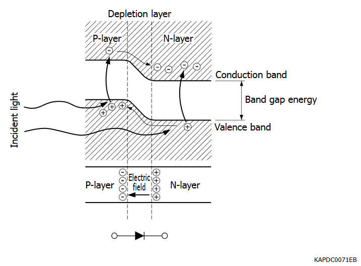
Figure 1-2 Visualization of silicon bandgap as the energy difference between valence and conduction bands
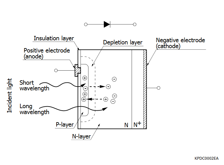
Figure 1-3 Absorption of shorter wavelengths vs. longer ones in a Si PN photodiode
However, if an external source of energy can be used to generate a surplus of charge carriers in either side of the depletion region, it is possible to disturb that equilibrium and induce a net current across the junction. That external source of energy could be thermal agitation (resulting in the so-called dark current) or the photoelectric effect if enough energy can be provided to an electron in the valence band to transition to the conduction band and leave a hole behind in the valence band (Figure 1-2). The resulting electron and hole are electrically compensated by each other (and not by any ion in the lattice); together, they are referred to as an electron-hole pair and are considered to be excess charge carriers.
Due to the presence of the depletion layer’s native E-field, once an excess electron-hole pair is formed in the depletion layer, each carrier type (electron or hole) drifts in opposite direction towards its majority side (N or P). That is because (by the laws of electrostatics) electrons, being negatively charged, must travel against the E-field’s direction (from the lower electrical potential of the depletion layer’s negative P side towards the higher potential of its positive N side) and holes, being positively charged, must travel in the E-field’s direction (from the higher electrical potential of the depletion layer’s positive N side towards the lower potential of its negative P side). In this process, only minority carriers (electrons generated in the depletion layer’s P side and holes generated in the layer’s N side) drift across the PN junction to arrive at the depletion layer’s outer edges; majority carriers (electrons generated in the layer’s N side and holes generated in the layer’s P side) do not cross the junction but drift to reach the layer’s outer edges.
After the excess electrons and holes reach the respective outer edge of the depletion layer, the electrons accumulate in the N region while the holes accumulate in the P region. Hence, if a current loop is formed between the P and the N regions in order to allow for the accumulated electrons and holes to travel to the opposite regions and recombine, photocurrent can flow in that loop (if the depletion layer is exposed to light photons of energies greater than the silicon band gap, which is 1.14 eV of energy difference between silicon’s conduction and valence bands). Certainly, the photoelectric effect can create electron-hole pairs outside the depletion layer as well, but most such pairs will have short lifetimes and undergo recombination before they can reach the depletion layer. That is due to poor collection efficiency in absence of an E-field outside the depletion layer since carriers would need to rely on diffusion and Brownian random walk to reach the layer (and then drift across the junction and be collected for readout).
The depletion layer’s depth affects the photosensitivity and frequency response of the PN photodiode. Longer light wavelengths are absorbed at deeper depths within silicon, and thus, enlarging the depletion layer’s depth increases the PN photodiode’s “red” photosensitivity (Figure 1-3). Also, analogous to increasing the distance in between the conducting plates of a parallel-plate capacitor, increasing the depletion layer’s depth decreases the PN junction’s capacitance, proportionally improving the PN photodiode’s frequency bandwidth (considering that is the frequency-domain electrical impedance of a capacitor). In either case, however, an increased depletion layer depth also results in greater collection of thermally-generated carriers that form a photodetector’s dark current. Nevertheless, many pulsed or red/NIR applications find a larger depletion depth to be beneficial in overall terms. For such applications, a PN photodiode’s depletion layer can be deepened by biasing the PN junction in reverse, which means biasing the N region (cathode) at a higher electric potential than the P region (anode). As the reverse bias voltage is increased in magnitude, the depletion layer’s depth can reach full depth of the photodiode’s bulk silicon, eliminating the loss of those photo-electrically generated carriers that would otherwise need to diffuse in order to reach the depletion layer and be collected.
Moreover, in order to further improve the frequency response and bandwidth of PN photodiodes, a region of intrinsic silicon can be introduced in between the P and N regions, forming a PIN photodiode. This intrinsic region results in a photodiode of smaller capacitance per unit of area, and thus, increased cutoff frequency and bandwidth. The intrinsic region’s role in decreasing junction capacitance can also be analogized to increasing the distance in between the conducting plates of a parallel-plate capacitor. This feature makes PIN photodiodes suitable for high-frequency pulsed applications that enjoy relatively abundant levels of light as PIN (and PN) photodiodes have no internal carrier multiplication or gain mechanism. These photodiodes operate at a gain of 1, and thus, they are suitable for detecting relatively strong light signals. With that, we will now proceed to discussing silicon photodetectors with internal gain mechanisms that are suitable for detecting lower light signal levels.
1-2. Avalanche photodiode (APD)
Aside from inducing deeper depletion, increasing the reverse bias voltage across a PN junction increases the electric force exerted on charge carriers (electrons and holes) by intensifying the E-field present in the depletion layer. Carriers accelerated by this force experience an increase in velocity and hence kinetic energy in between scattering collisions with atoms (whether silicon or dopant) in the crystal’s lattice. Such collisions result in loss of carrier kinetic energy through thermal vibration of the crystal lattice (referred to as phonon vibration). However, if the E-field’s strength is such that mean energy of carriers can exceed the silicon band gap energy during their average travel time in between consecutive collisions, sufficiently-energetic carriers emerge that are likely to ionize lattice atoms upon impact and release at least another electron-hole pair into conduction and valence bands per impact. This impact ionization effect constitutes a carrier multiplication phenomenon by which the number of drifting carriers increases rapidly, resembling an avalanche. The extent of that increase in carrier population between the original photo-carrier count and the final charge signal collected and read out is the gain of the avalanche process.
The sole benefit of avalanche gain is to increase the magnitude of the original photoelectric signal (with respect to its own inherent noise) to a level that can adequately surpass the noise floor of the readout mechanism (typically an amplifier circuit). However, since carrier multiplication in terms of E-field acceleration time/distance and energy losses to phonon collisions has an inherent randomness, the avalanching carriers develop a fluctuating spread of energies and hence multiplication gains during the avalanche process. That in turn contributes an excess noise factor (Figure 1-4) to the original signal as a random fluctuation in the APD’s overall internal gain. Despite this multiplication excess noise factor, many mid-to-low light level applications nonetheless find the APD and its internal gain greatly beneficial. APD gain is dependent on the incident light wavelength (Figures 1-5, 1-6) and increases with reverse bias voltage (Figure 1-7). Furthermore, the gain diminishes with temperature (due to increased phonon vibrations at higher temperatures and thus greater losses in kinetic energies of avalanching carriers due to increased scattering collisions) as shown in Figure 1-8.

Figure 1-4 Plots of excess noise factor vs. gain at three different wavelengths for a Hamamatsu APD
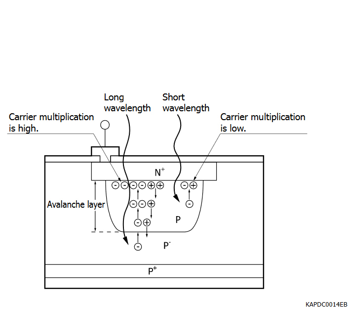
Figure 1-5 Visualization of absorption of short and long wavelengths of light in a red/NIR-enhanced N-on-P APD structure
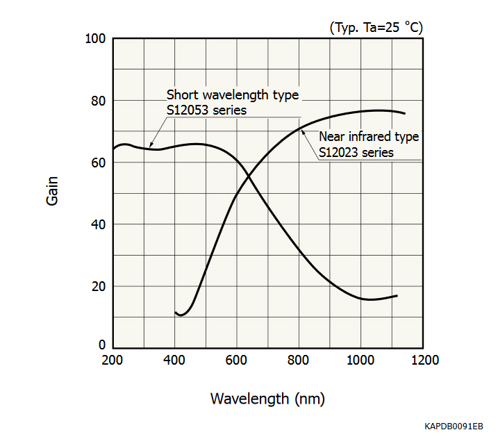
Figure 1-6 Gain dependence on incident light wavelength for two Hamamatsu APDs
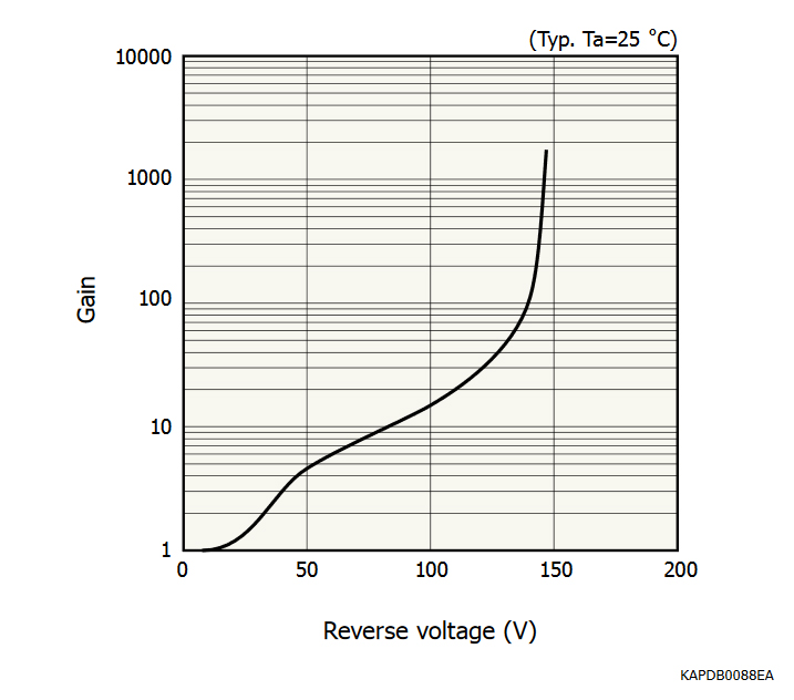
Figure 1-7 Plot of APD gain vs. reverse bias voltage
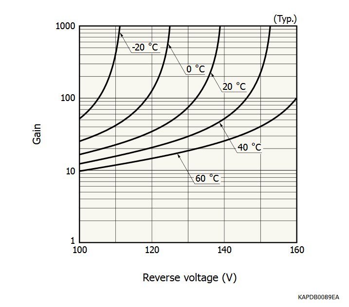
Figure 1-8 Effects of temperature on gain vs. reverse voltage
Amongst the above APD gain characteristics, a peculiarly curious case is the gain’s dependence on wavelength; to see why, we should note that an APD can be fabricated in two alternative structures: N-on-P and P-on-N. The N-on-P structure offers greater gain and enhanced photosensitivity in response to longer wavelengths (at the expense of shorter ones) while the P-on-N structure has higher gain and photosensitivity in response to shorter wavelengths (at the expense of longer ones). This difference in structure also pertains to the MPPC as well but only affects its photosensitivity; we will revisit and explain these structures as part of our discussion of the MPPC.
Another particularly interesting characteristic is APD gain’s dependence on applied reverse voltage as shown in Figure 1-7. Based on the two knees of the plot in Figure 1-7 and the three resulting gain vs. reverse voltage regions, APD gain demonstrates three distinct behaviors with respect to reverse voltage. In the example plot shown in Figure 1-7, those distinct behaviors are (A) below about 50 V, (B) between around 50 V and about 100 V, and (C) above 100 V. For the sake of our discussion, we will address the latter two. By fitting a trend line, we observe that gain approximately has a 10αV relationship with reverse voltage under the moderate electric field intensities of region (B) but increases very steeply with reverse voltage in region (C). The steep slope of region (C) poses a concern to the use of the APD in photometric applications, since it raises the question of whether the APD’s internal gain can be reliably controlled and accurately known in region (C) or not; a stable and reliably controllable gain is essential to a deterministic relationship between input and output of a detector used in a measurement. In other words, accurate determinability of APD gain is critical to its application in high-accuracy measurements. Moreover, a stable gain is a fundamental aspect of maintaining the APD’s overall response linearity.
We thus proceed to demonstrate that the APD’s avalanche gain response is theoretically linear. Although a comprehensive mathematical formulation of the avalanche process is quite complex, to illustrate that linearity in the simplest way possible, let’s say a single photon generates an initial photoelectron and hole pair that mutually succeeds at impact ionization and creating two electron-hole pairs. In our simplified example, if electrons and holes have the same fixed ionization probability of P to generate only one electron-hole pair per ionization, we can characterize the avalanche process as forming (if n ? 8) avalanching carriers in average where i = 0, 1, 2, 3, ... represents the sequential iterations of carrier multiplication. Now, if we increase the initial number of photoelectrons and holes triggering the avalanche to 2m (created by m > 1 detected photons), the count of avalanching carriers after n ? 8 iterations of carrier multiplication would be . We thus observe that the ratio between the two final avalanche populations is m, and therefore, there exists a linear relationship of proportionality by a factor of m between the two final populations (one of which was originated by 1 photon and the other by m photons).
Another noteworthy conclusion from the above simplistic model is that the APD’s gain (as the ratio of the avalanche’s final carrier population to its initial carrier population) is , which means that if P ? 1 under a sufficiently-intense E-field, the APD’s gain approaches infinity. Nonetheless, the APD nature is actually more complex in nature than our simplistic model above: avalanching electrons and holes ionize atoms at differing probabilities under moderate E-field intensities; those differing ionization probabilities increase significantly and converge as the electric field intensifies to higher levels. Without delving into its complicated mathematical derivation, the APD’s gain as a carrier multiplication factor can be formulated as in which and are the ionization efficiencies (probabilities per unit of travelled distance) of avalanching electrons and holes, k is the ratio of ionization efficiency of a hole to that of an electron , and d is the thickness of the avalanche layer depicted in Figure 1-9; it is the distance within the APD’s depletion layer over which the E-field is strong enough for the avalanche process to occur. Plots of ionization efficiencies of electrons and holes and their dependencies on E-field intensity within the depletion layer have been shown for silicon in Figure 1-10.
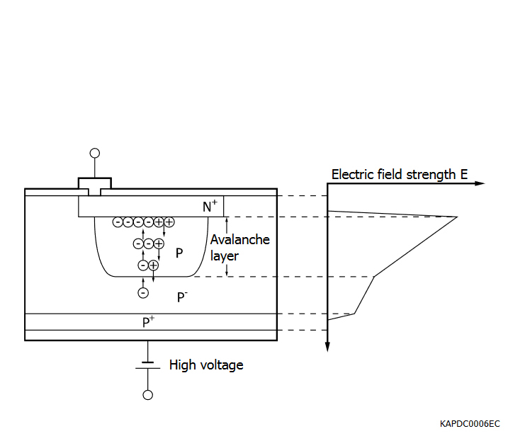
Figure 1-9 The avalanche region within a Si APD
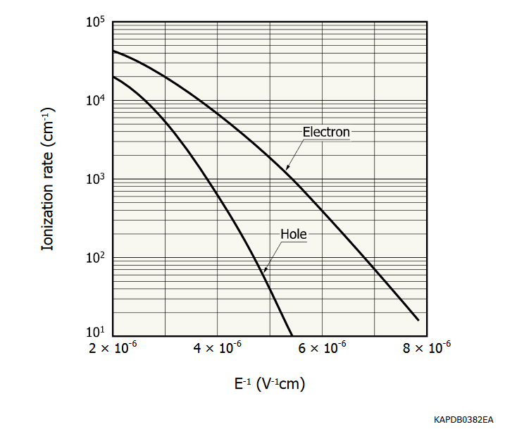
Figure 1-10 Ionization efficiencies of electrons and holes drifting under an electric field in silicon at 300 K
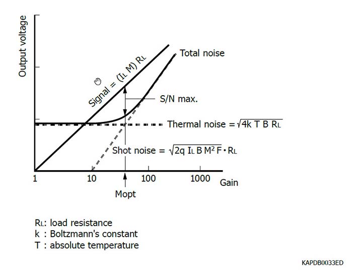
Figure 1-11 Practical determination of an APD’s optimal gain
In our theoretical study of APD gain, three specific scenarios are of interest:
- Optimal APD gain is the highest gain level at which the APD maintains relatively constant bandwidth and stable noise output; theoretically, that optimal gain is , and assuming , it is attained once the condition is met. However, since measurement of carrier ionization efficiencies in a specific APD and monitoring the establishment of the aforementioned condition are not trivial tasks, the optimal gain can instead be determined by the approach depicted in Figure 1-11. APD gain is typically on the order of few 10 up to 100 for optimal operation.
2 Derivation:
- For M ? 8, we have , which leads to . If this theoretical condition is met between and over the range of d, the APD is said to be in breakdown; the reverse bias voltage at which this phenomenon (M ? 8) occurs is referred to as the APD’s breakdown voltage.
- A practical breakdown scenario occurs after the reverse bias voltage increases to a point that causes k ? 1 and thus results in . Consequently, if the bias voltage (or further increase thereof) results in , we will have M ? 8. Based on the data plot in Figure 1-10, k ? 1 occurs when the ionization efficiencies converge to an order of magnitude of around at an E-field intensity of about (corresponding to a reverse bias voltage on the order of 100 V across a 10 µm-deep depletion layer).
In technical terminology, operating an APD in the breakdown state (i.e. the applied reverse bias voltage being higher than the APD’s breakdown voltage) is referred to as Geiger-mode operation.
Now, recall our earlier discussion of Figure 1-7 (APD gain vs. reverse voltage plot) and the issue of APD gain stability and linearity in “operation region (C)” in which APD gain shoots up towards higher and higher values. That issue indeed applies to a Geiger-mode avalanche whose output charge (per avalanche) is the same for a given gain and its corresponding reverse bias voltage regardless of the initial number of photo-carriers that initiated it (contrary to the linear APD response that we described with a simplistic model earlier). This makes an APD operating in the Geiger mode to be a so-called digital photodetector (as opposed to being linear or analog), since it lacks a linear response between its input (i.e. detected amount of light) and output (i.e. amount of outputted charge); its response is indeed a binary one, corresponding to signal detection or lack thereof.
Since a single photoelectron-hole pair is all that is needed to trigger a Geiger-mode avalanche, APD gain in the Geiger mode for a given bias voltage can be obtained by dividing its output charge by the fundamental charge of an electron. Without delving into its detailed derivation, output charge of a Geiger avalanche is the product of the APD’s junction capacitance and the applied operating overvoltage (i.e. difference between the applied reverse bias voltage and the APD’s breakdown voltage VBR). Thus, we can formulate the APD’s Geiger-mode gain as: . In a typical APD, depending on its surface area, the junction capacitance is on the order of several 10 to a few 100 pF while is 1.6 ×10⁻¹⁹ C. Thus, it can be concluded from this equation and by the large ratio of that biasing an APD in Geiger-mode requires an ultralow-ripple power supply in order to attain good gain stability.
Another peculiar aspect of Geiger-mode operation is the population density of avalanching carriers in the depletion region. In Geiger mode, this density reaches such high levels that the cloud of avalanching carriers behaves like a conductor with very low resistance under a finite bias voltage. This results in a surge of current through the APD that by intense generation (through scattering collisions) and recombination continually mobilizes valence electrons from high energy states susceptible to contributing to the avalanche multiplication process, rendering the APD unable to produce discrete output pulses. It is thus necessary to quench that current surge once sufficient gain and adequate output signal amplitude have been attained so that a subsequent photoelectron event can lead to a succeeding output pulse. Figure 1-12 shows the equivalent circuit of a Geiger-mode APD (GAPD) and can be used to describe how that quenching is performed.
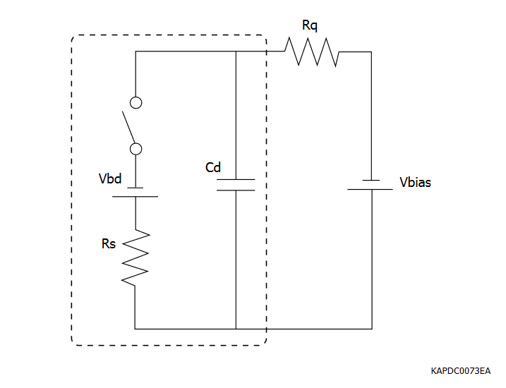
Figure 1-12 Equivalent circuit of a Geiger-mode APD (GAPD)
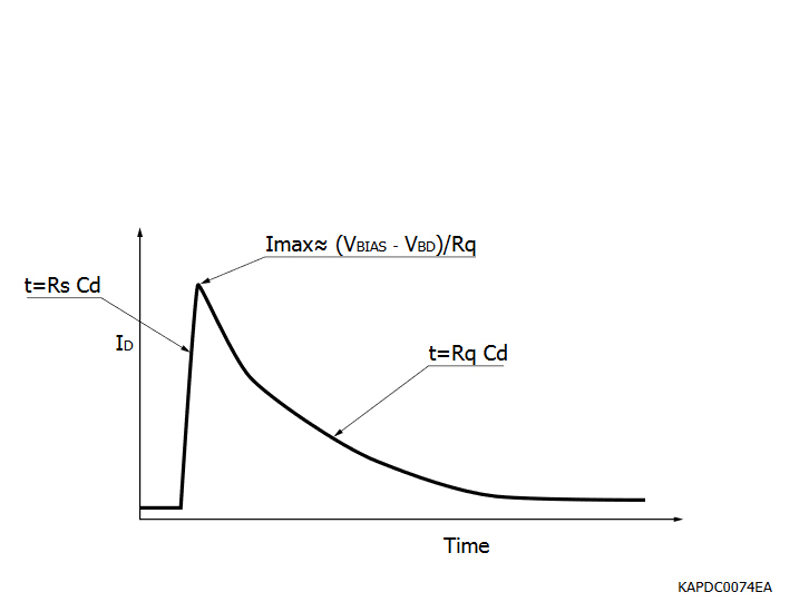
Figure 1-13 Conceptual output pulse of the equivalent circuit
In this equivalent circuit, the GAPD capacitance (Cd) is initially biased at Vbias while the conceptual switch shown is open. Once an electron-hole pair is generated within the depletion layer (whether thermally or by the photoelectric effect), the conceptual switch closes, and Cd begins to discharge through GAPD’s series resistance (Rs), whose small value (diminished by the avalanching carrier population) provides for a surge in current flow while the potential difference across Cd (let’s call it Vd) exponentially decays towards the breakdown voltage (Vbd). This decline in Vd weakens the avalanche process, increasing Rs and decreasing Cd’s discharge current flow. Based on the GAPD equivalent circuit’s two current loops, the following relationship can be established to describe the net current flow through .
Since the current flows in the two loops would be in opposite directions (one entering Cd to recharge it and another leaving Cd to discharge it), net current Id would flow in the direction of the stronger current flow. Thus, if at point where Vd is such that Vd-Vbd=Vbias-Vd, the quenching resistor Rq is so small that a recharge current continues to flow into Cd and sustains its discharge through Rs, the quenching process shall not take place. However, if Rq is large enough so that the current flow from Vbias cannot sustain Cd’s discharge, the avalanche process would be quenched. Thus, once the discharge is exhausted and reaches its trough, the avalanche process is quenched and the conceptual switch opens. The recharge current flowing into Cd through Rq increases the voltage across Cd by Vbias-Vbd to equal Vbias, preparing the GAPD for the next avalanche. It should be noted that Rq values large enough to facilitate the quenching process are generally determined empirically.
The recharge process of Cd is commonly called recovery and its time duration is generally characterized by the time constant Rq • Cd. During the brief period of avalanche multiplication (corresponding to the fast time constant Rs • Cd and the subsequent recovery time, a GAPD is rather unavailable to detect a new photoelectric event; any output pulse meanwhile generated would practically have a small amplitude (depending on the remaining amount of Cd’s stored charge that is available for a secondary discharge). To decrease the GAPD’s recovery time (Figure 1-14), its net capacitance can be reduced by theoretically introducing a smaller capacitance in series with Cd as part of the readout scheme; the resulting decrease in recovery time comes with a tradeoff of lower overall gain due to a reduced net capacitance (since gain is proportional to GAPD’s capacitance as described earlier). From a practical circuit design standpoint, this theoretical arrangement can be implemented by introducing a high-pass filter with a CR time constant desirably shorter than GAPD’s recovery time at the input of the amplifier circuit used for the GAPD’s readout [Figure 1-15]. The amplifier output pulse is thus shaped such that net overall gain loss is in which fC is the filter’s cutoff frequency and fGAPD is the frequency bandwidth of GAPD’s recovery while the amplifier output pulse’s fall time (90% to 10% of amplitude) can be obtained as the RMS of the amplifier’s and the GAPD’s fall times to be or considering that and that fall time of a CR circuit is approx. 2.2 times its time constant.
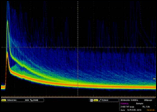
Figure 1-14a Shaping the output pulse of a GAPD in order to decrease its recovery time (MPPC: 3×3 mm) - (a) Before
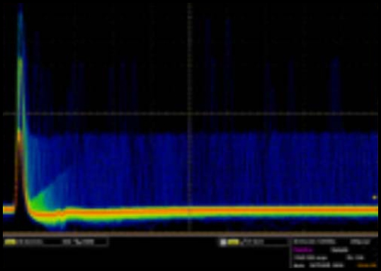
Figure 1-14b Shaping the output pulse of a GAPD in order to decrease its recovery time (MPPC: 3×3 mm) - (b) After
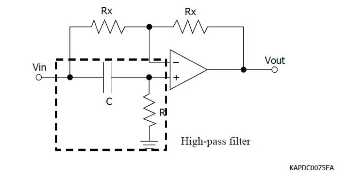
Figure 1-15 Amplifier circuit diagram with high-pass filter
The exceedingly high levels of avalanche gain (on the order of several 105 to 106) in Geiger mode make this APD operation regime particularly interesting to applications with low light levels; specialized GAPDs have been developed for utilization in such applications. However, in order to overcome GAPD’s unavailability for photoelectron detection during its recovery time and to address its lack of a linear response, a far more versatile category of silicon photodetectors has been developed based on the GAPD concept by arranging a matrix of them within the same field-of-view of the incident light signal. We will now proceed to learn about the multi-pixel photon counter or MPPC.
1-3. MPPC (multi-pixel photon counter)
Also known as silicon photomultiplier or SiPM, the MPPC is a common-bias and common-output (common-cathode) matrix of GAPD elements (called pixels or microcells) connected in parallel and fabricated on a monolithic silicon crystal. Figures 1-16, 1-17, and 1-18 illustrate the layout of MPPC pixels.
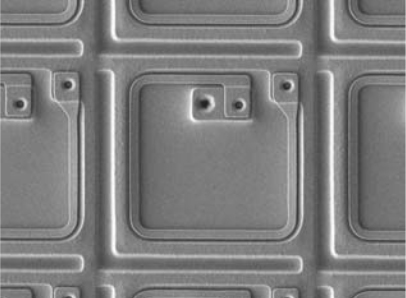
Figure 1-16a Pixel pitch: 25 µm - Individual MPPC pixels (microcells) with a metal-composite quenching resistor fabricated around each microcell
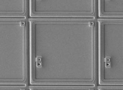
Figure 1-16b Pixel pitch: 50 µm - Individual MPPC pixels (microcells) with a metal-composite quenching resistor fabricated around each microcell
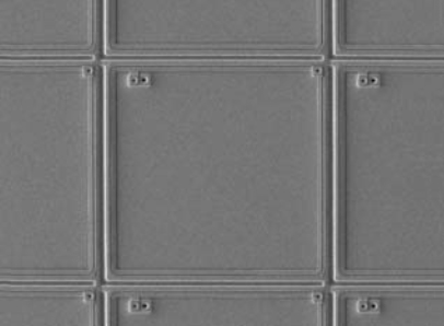
Figure 1-16c Pixel pitch: 75 µm - Individual MPPC pixels (microcells) with a metal-composite quenching resistor fabricated around each microcell
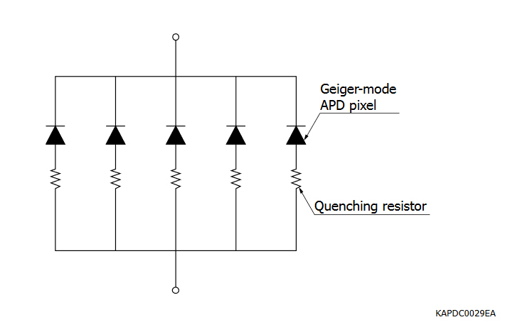
Figure 1-17 Conceptual illustration of the MPPC as a matrix of GAPD pixels (microcells) connected in parallel
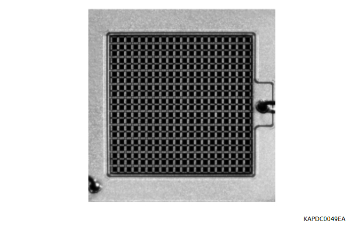
Figure 1-18 An actual matrix implementation of MPPC microcells
Similar to the APD, a MPPC pixel can be fabricated based on two distinct structures: N-on-P (for enhanced red/NIR photosensitivity) and P-on-N (for enhanced UV/blue photosensitivity).
The difference in photosensitivity of these structures is caused by how much farther an electron, which has greater ionization efficiency and hence avalanche probability in silicon than a hole, must travel within the depletion layer before being collected. In the N-on-P structure, longer light wavelengths create an electron-hole pair in the P region due to such wavelengths’ greater absorption depths in silicon. On the other hand, in the P-on-N structure, shorter wavelengths create an electron-hole pair also in the P region due to such wavelengths’ shallower absorption depths in silicon. As explained in our discussion of a PN photodiode’s operation, a photoelectron generated in the depletion layer’s P side is swept across the PN junction in the opposite direction of the depletion layer’s E-field. Prior to collection, that electron would consequently face a longer pathlength, which, combined with its higher ionization efficiency and avalanche probability, leads to a greater likelihood of avalanche initiation and hence detection.
The MPPC has a set of fundamental characteristics that are shown in the plots of Figures 1-19 to 1-22.
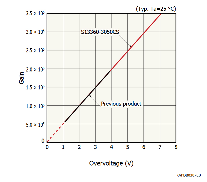
Figure 1-19 Gain vs. overvoltage (S13360-3050CS)
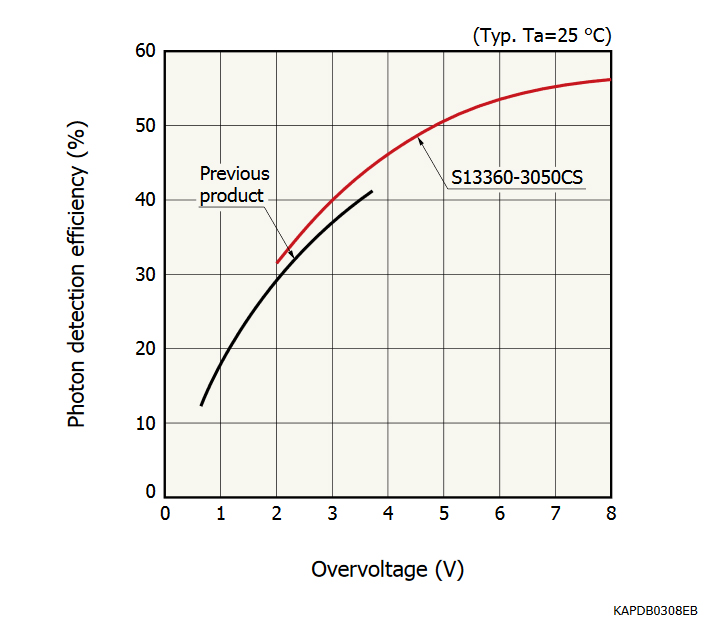
Figure 1-20 PDE vs. overvoltage (S13360-3050CS)
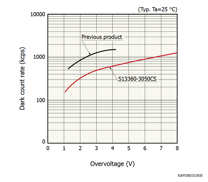
Figure 1-21 Dark count rate vs. overvoltage (S13360-3050CS)
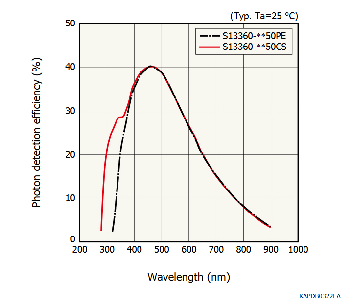
Figure 1-22 PDE vs. wavelength (S13360 series)
Some MPPC characteristics are dependent on temperature. Of particular note are the temperature dependencies of photon detection efficiency (PDE), gain, and dark count rate (DCR). MPPC’s PDE is the product of silicon’s quantum efficiency (QE) times MPPC pixel fill-factor (ratio of pixel photosensitive area to total area) times Geiger-mode avalanche probability. Silicon’s QE increases at elevated temperatures due to increased phonon vibrations: those vibrations facilitate the transition of electrons to the conduction band and the formation of holes in the valence band and thus improve silicon’s photosensitivity (although, that facilitation pertains not only to photo-carriers but also to thermal carriers that constitute a silicon photodetector’s dark current). However, avalanche probability has a decreasing relationship with increased temperature, countering QE’s increasing relationship with temperature. As a result, MPPC’s PDE is affected by the more dominant of these opposing factors as temperature changes and could even remain stable over some ranges of temperature.
Like in the case of the APD, in absence of temperature control, the MPPC’s biasing scheme requires a temperature-compensation circuit that would adjust the applied bias voltage with changes in temperature in order to maintain a constant MPPC gain. Also, like in the case of the APD, MPPC gain declines with increases in temperature due to increased phonon vibrations at higher temperatures and thus greater scattering collisions and losses in kinetic energies of avalanching carriers; based on our earlier definition of GAPD gain, this decline in gain stems from an increasing breakdown voltage as temperature increases.
Being a noise that occurs randomly and uncorrelated with photon-initiated output pulses, DCR is detrimental to utilizing the MPPC for single-photon counting applications. However, if the time window during which single photon events are most likely to occur is sufficiently narrow and can be known to the detector system by availability of an external trigger, DCR is no longer detrimental to single-photon counting with the MPPC. For example, if the time window in question is 10 ns in duration, the likelihood of a single dark count at DCR = 1000 kcps (cps: counts per second) occurring during that time window is fairly slim, and it therefore becomes possible to detect single photons using the MPPC with a high degree of statistical confidence. Nevertheless, if the above timing constraints on single-photon events cannot be met, DCR can be reduced by thermoelectric cooling of the MPPC at a rate of about 1/2 for every approx. 10 ºC reduction in temperature as shown in Figure 1-23.
On the other hand, in applications with several photons or more per light event, DCR can be excluded from readout by increasing the discriminator level. As a general rule of thumb, for every one single-photoelectron (1 p.e.) output pulse height increase in the discriminator’s threshold level, DCR readout diminishes by about an order of magnitude as shown in Figure 1-24.
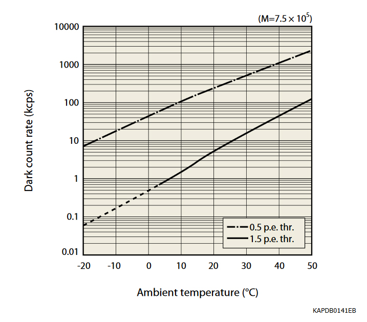
Figure 1-23 A typical MPPC’s DCR vs. temperature
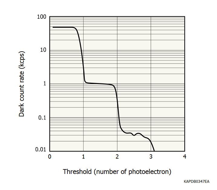
Figure 1-24 DCR vs. counting discriminator threshold level
In addition to DCR, MPPC operation has two peculiar types of noise that are correlated in occurrence with detection of photon signal and deserve individual discussion:
i. Afterpulses: During an avalanche process (whether triggered by a photoelectron or a thermal carrier), a small portion of avalanching carriers get trapped in impurity energy levels but are released after short delays (typically on the order of few 1-10 ns) upon receiving the required energy (albeit small) to reenter the conduction or valence band. Upon their release, these carriers initiate new avalanche pulses, which appear with delays after the genuine parent pulse and are hence referred to as afterpulses. Please see Figure 1-27 for a waveform showing strong afterpulsing. If an afterpulse is released during the MPPC pixel’s recovery time, its amplitude will be shorter than that of a regular (1 p.e.) pulse and can thus be discriminated against by pulse-height analysis (PHA) and excluded from data processing. However, if the afterpulse is released after the MPPC pixel’s recovery, it will have a full (1 p.e.) pulse amplitude and will be indistinguishable in amplitude or shape from a genuine output pulse. In ultralow DC light level applications where consecutive single-photon events in close timing proximity are unlikely or in ultralow-rate pulsed applications (where time differences between succeeding pulses are large) or when the timing of a pulse can be known by availability of a trigger (regardless of what the pulse rate might be), a time-delay filtering algorithm could be used to exclude full-height afterpulses. Nevertheless, Hamamatsu MPPCs have greatly diminished levels of afterpulsing as shown in Figure 1-26.
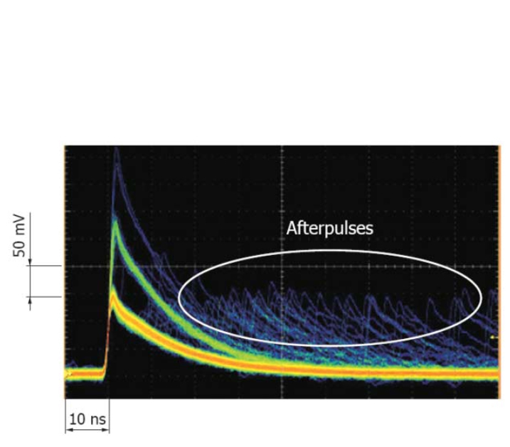
Figure 1-25 Waveform showing the occurrence of afterpulses
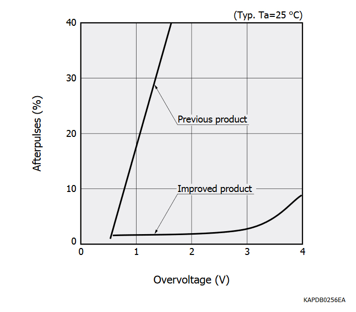
Figure 1-26 Much reduced afterpulsing of Hamamatsu MPPC
ii. Optical crosstalk: During the avalanche process, kinetic energy of avalanching carriers (even if larger than silicon’s band gap energy) need not necessarily contribute to carrier multiplication. As discussed earlier, through scattering collisions, a portion of that energy is lost as heat to phonon vibrations. In a less likely phenomenon, it is also possible for that energy to be emitted as photons. When that occurs, the resulting photons can travel to the neighboring MPPC pixels and initiate avalanches in them. This undesirable phenomenon is referred to as optical crosstalk. If a crosstalk photon produces an electron-hole pair in the depletion layer of a neighboring pixel and triggers an avalanche process as a result, this situation is called prompt crosstalk, whose output pulse appears simultaneously with the genuine original pulse. Please see Figure 1-27 for a waveform showing strong prompt optical crosstalk. With the exception of using an upper-level discriminator in single-photon counting, there is unfortunately no way to discriminate against prompt crosstalk pulses in order to exclude them from data processing. However, in the alternative scenario that the crosstalk photon creates an electron-hole pair outside an MPPC pixel’s depletion layer, the resulting electron-hole pair can only trigger an avalanche process after successfully (albeit improbably) reaching the depletion layer by diffusion. This introduces a delay between the original pulse and its crosstalk noise, which is called delayed crosstalk. Delayed crosstalk can be excluded by the same approach as for excluding full-height afterpulses.
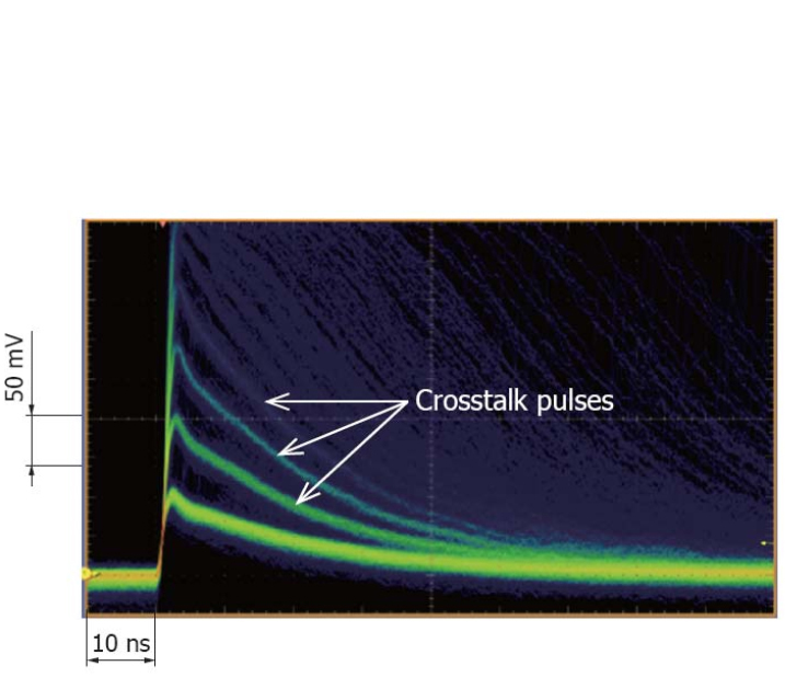
Figure 1-27 Waveform showing the occurrence of prompt crosstalk
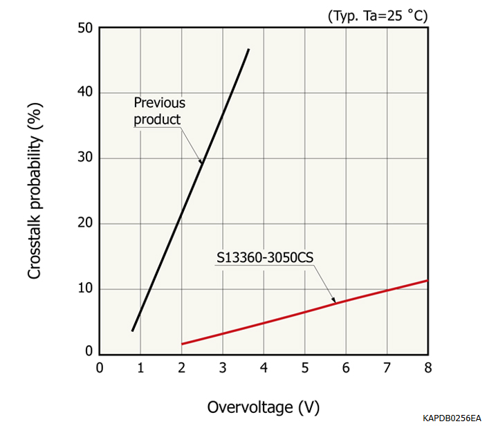
Figure 1-28 Much reduced crosstalk of Hamamatsu MPPC
Note: Dark pulse overlap (pileup effect) is eliminated.
Consequently, (prompt) crosstalk is a particularly detrimental source of noise to applications with ultralow-level light signals (such as multi-photon counting). As shown in Figure 1-28, however, Hamamatsu MPPCs enjoy substantially diminished levels of crosstalk, thanks to optical trenches that are implemented around every MPPC pixel in order to block crosstalk photons from reaching neighboring pixels. Furthermore, considering that optical crosstalk is correlated with signal detection and increases with gain (as an indicator of the intensity of the avalanche process and its byproduct photons), operation of the MPPC at a lower gain while maintaining a higher overvoltage and hence PDE is essential to overcoming the detrimental impact of crosstalk in low-signal applications. Since gain is directly proportional to both overvoltage and also MPPC pixel capacitance while PDE takes no effect from pixel capacitance, it becomes of paramount importance to select MPPCs with low pixel capacitance for low-signal applications.
Our discussion of characteristics of silicon photodetectors, including the MPPC, has been qualitative so far. However, in order to select suitable photodetectors for practical real-world applications, it is necessary to develop a quantitative framework to assess photodetector performance under an application’s conditions. In the following sections 2 and 3, we will discuss generalized quantitative methods for selection of silicon APD and MPPC products for a broad range of applications. A primary objective has been to describe methods that could be used for any application as long as certain basic pieces of information are available about the application; these methods could be used for photodetector selection consistently, regardless of the particular application involved. However, it is important to note that the methods described are meant to serve as preliminary and general guidelines (so-called back-of-the-envelope calculations); they are intended to serve as early indicators of what product(s) to begin considering. As the design and development works advance, these methods would not substitute extensive simulation and comprehensive evaluation under the application’s specific conditions. With this understanding, let’s now proceed to discussing preliminary calculation methods for assessing APD and MPPC performance.
- Confirmation
-
It looks like you're in the . If this is not your location, please select the correct region or country below.
You're headed to Hamamatsu Photonics website for US (English). If you want to view an other country's site, the optimized information will be provided by selecting options below.
In order to use this website comfortably, we use cookies. For cookie details please see our cookie policy.
- Cookie Policy
-
This website or its third-party tools use cookies, which are necessary to its functioning and required to achieve the purposes illustrated in this cookie policy. By closing the cookie warning banner, scrolling the page, clicking a link or continuing to browse otherwise, you agree to the use of cookies.
Hamamatsu uses cookies in order to enhance your experience on our website and ensure that our website functions.
You can visit this page at any time to learn more about cookies, get the most up to date information on how we use cookies and manage your cookie settings. We will not use cookies for any purpose other than the ones stated, but please note that we reserve the right to update our cookies.
1. What are cookies?
For modern websites to work according to visitor’s expectations, they need to collect certain basic information about visitors. To do this, a site will create small text files which are placed on visitor’s devices (computer or mobile) - these files are known as cookies when you access a website. Cookies are used in order to make websites function and work efficiently. Cookies are uniquely assigned to each visitor and can only be read by a web server in the domain that issued the cookie to the visitor. Cookies cannot be used to run programs or deliver viruses to a visitor’s device.
Cookies do various jobs which make the visitor’s experience of the internet much smoother and more interactive. For instance, cookies are used to remember the visitor’s preferences on sites they visit often, to remember language preference and to help navigate between pages more efficiently. Much, though not all, of the data collected is anonymous, though some of it is designed to detect browsing patterns and approximate geographical location to improve the visitor experience.
Certain type of cookies may require the data subject’s consent before storing them on the computer.
2. What are the different types of cookies?
This website uses two types of cookies:
- First party cookies. For our website, the first party cookies are controlled and maintained by Hamamatsu. No other parties have access to these cookies.
- Third party cookies. These cookies are implemented by organizations outside Hamamatsu. We do not have access to the data in these cookies, but we use these cookies to improve the overall website experience.
3. How do we use cookies?
This website uses cookies for following purposes:
- Certain cookies are necessary for our website to function. These are strictly necessary cookies and are required to enable website access, support navigation or provide relevant content. These cookies direct you to the correct region or country, and support security and ecommerce. Strictly necessary cookies also enforce your privacy preferences. Without these strictly necessary cookies, much of our website will not function.
- Analytics cookies are used to track website usage. This data enables us to improve our website usability, performance and website administration. In our analytics cookies, we do not store any personal identifying information.
- Functionality cookies. These are used to recognize you when you return to our website. This enables us to personalize our content for you, greet you by name and remember your preferences (for example, your choice of language or region).
- These cookies record your visit to our website, the pages you have visited and the links you have followed. We will use this information to make our website and the advertising displayed on it more relevant to your interests. We may also share this information with third parties for this purpose.
Cookies help us help you. Through the use of cookies, we learn what is important to our visitors and we develop and enhance website content and functionality to support your experience. Much of our website can be accessed if cookies are disabled, however certain website functions may not work. And, we believe your current and future visits will be enhanced if cookies are enabled.
4. Which cookies do we use?
There are two ways to manage cookie preferences.
- You can set your cookie preferences on your device or in your browser.
- You can set your cookie preferences at the website level.
If you don’t want to receive cookies, you can modify your browser so that it notifies you when cookies are sent to it or you can refuse cookies altogether. You can also delete cookies that have already been set.
If you wish to restrict or block web browser cookies which are set on your device then you can do this through your browser settings; the Help function within your browser should tell you how. Alternatively, you may wish to visit www.aboutcookies.org, which contains comprehensive information on how to do this on a wide variety of desktop browsers.
5. What are Internet tags and how do we use them with cookies?
Occasionally, we may use internet tags (also known as action tags, single-pixel GIFs, clear GIFs, invisible GIFs and 1-by-1 GIFs) at this site and may deploy these tags/cookies through a third-party advertising partner or a web analytical service partner which may be located and store the respective information (including your IP-address) in a foreign country. These tags/cookies are placed on both online advertisements that bring users to this site and on different pages of this site. We use this technology to measure the visitors' responses to our sites and the effectiveness of our advertising campaigns (including how many times a page is opened and which information is consulted) as well as to evaluate your use of this website. The third-party partner or the web analytical service partner may be able to collect data about visitors to our and other sites because of these internet tags/cookies, may compose reports regarding the website’s activity for us and may provide further services which are related to the use of the website and the internet. They may provide such information to other parties if there is a legal requirement that they do so, or if they hire the other parties to process information on their behalf.
If you would like more information about web tags and cookies associated with on-line advertising or to opt-out of third-party collection of this information, please visit the Network Advertising Initiative website http://www.networkadvertising.org.
6. Analytics and Advertisement Cookies
We use third-party cookies (such as Google Analytics) to track visitors on our website, to get reports about how visitors use the website and to inform, optimize and serve ads based on someone's past visits to our website.
You may opt-out of Google Analytics cookies by the websites provided by Google:
https://tools.google.com/dlpage/gaoptout?hl=en
As provided in this Privacy Policy (Article 5), you can learn more about opt-out cookies by the website provided by Network Advertising Initiative:
http://www.networkadvertising.org
We inform you that in such case you will not be able to wholly use all functions of our website.
Close