Application notes
Technical notes
Ask an engineer
Publications
United States (EN)
Select your region or country.
What is an SiPM and how does it work?
Slawomir Piatek, PhD, Hamamatsu Corporation & New Jersey Institute of Technology
October 7, 2016
- What is a silicon photomultiplier?
- How does a SiPM work?
- Gain of a silicon photomultiplier
- What is the photon detection efficiency (PDE) of a SiPM?
- How to measure breakdown voltage in a SiPM
- S/N in a continuous wave operation of a SiPM
- Optical crosstalk in a SiPM
- Measuring crosstalk probability in a SiPM
- References
- About the author
Related content: A technical guide to silicon photomultipliers (MPPC)
What is a silicon photomultiplier?
A silicon photomultiplier (SiPM) is a solid-state photodetector that in response to absorption of a photon can produce a current pulse several tens nanoseconds long containing 105 to 106 electrons. Therefore, a SiPM has a gain. This gain is comparable to that of a photomultiplier tube (PMT).
Structure
A SiPM is a pixelated device where each pixel, or a microcell, is a series combination of an avalanche photodiode (APD) and a quenching resistor (RQ). All of the microcells are connected in parallel; thus, a SiPM has two prongs: an anode and a cathode. The three panels in the figure below show, from left to right, a cross section of three microcells in a possible architecture, top view — the side of impinging light — of the device, and an equivalent electrical circuit.

Figure 1. This figure depicts a typical structure of a SiPM. It does not correspond to the actual structure of the Hamamatsu product.
In practical SiPMs, the microcells of identical size are arranged in a rectangular pattern. Depending on the device, the size of a microcell varies from 10 μm to 100 μm and the number of microcells per device ranges from several hundreds to several tens of thousands. SiPMs have active areas ranging from 1 mm2 to 6 mm2 and spectral sensitivities from UV to IR, peaking in the visible (400 nm - 500 nm).
Operation
A SiPM is externally biased so that the voltage on each APD is above its breakdown voltage. Thus each APD operates in Geiger mode. The difference between the biasing voltage and the breakdown voltage is known as overvoltage — the main adjustable parameter controlling operation of the device. If a SiPM absorbs a photon, the resulting charge carrier (an electron or hole depending on the structure) can trigger an avalanche in the gain region (shown as the gray oval in the figure) within the p+ - n+ structure. The avalanche can produce 105 - 106 carriers; this constitutes the gain. The role of the quenching resistor is to restore the APD back to the Geiger mode. The gain of a SiPM depends linearly on the overvoltage and the value of junction capacitance. Even though a SiPM is a pixelated device, it is not an image sensor. It does not store charge like a CCD does. It is an analog device producing a time-varying output signal that is measured in real time.
Characteristics
There are several key parameters characterizing a SiPM. These are breakdown voltage, gain versus overvoltage relation, photon detection efficiency, crosstalk probability, afterpulsing probability, and dark count rate.
Applications
A SiPM most resembles a PMT in its operation and characteristics. Compared to a PMT, a SiPM requires a lower operating voltage; has immunity to magnetic fields; is sturdier and more rugged; and is smaller in size. For these and other reasons, the SiPM has begun to replace PMTs in low-light applications such as positron emission tomography (PET), light detection and ranging (LIDAR), or radiation detection in high-energy physics.
How does a SiPM work?
A silicon photomultiplier (SiPM), though pixelated, is a photodetector that produces an analog output signal in real time. The output is a time sequence of waveforms (or current pulses), which have a discrete distribution of amplitudes: A, 2A, 3A, etc. The histogram of the amplitudes depends on the intensity and time-characteristics of the incident light. This note is a closer look into how a single microcell of a SiPM generates a waveform in response to light.
Operation
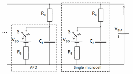
Figure 2. A simplified equivalent circuit of a SiPM (two representative microcells) biased with an external voltage source VBIAS.
All of the microcells in Figure 2 are in parallel. A microcell is a series combination of an avalanche photodiode (APD) and a quenching resistor RQ. The circuit modeling the APD is a parallel combination of a capacitor CJ (representing the junction capacitance) with a series combination of a switch S, voltage source VBD (equal to the breakdown voltage), and a resistor RS (representing the resistance of the entire APD during a discharge).
In the absence of light and ignoring dark counts, S is open and the voltage on CJ is VBIAS (VBIAS > VBD) — the microcell is in a light-sensitive state and the APD is in Geiger mode. When the microcell absorbs a photon, an electron-hole pair forms; one of the charge carriers drifts to the avalanche region, where it can initiate an avalanche. At the instant the avalanche begins, S closes causing CJ to be discharging through RS (RS ≪ RQ) with the time constant RSCJ. The voltage on CJ decreases, lowering the probability of impact ionization. For optimal RQ, the probability eventually becomes so small that the avalanche quenches. At this moment, S opens and VBIAS recharges CJ with the time constant RQCJ.
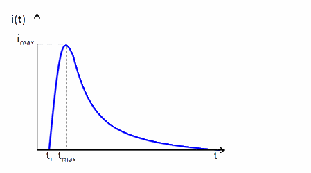
Figure 3. A graph of the current flowing through the terminals of the SiPM during the process discussed above.
In Figure 3, the avalanche begins at ti and quenches at tmax. The leading edge of the pulse starts at ti and the rise is proportional to . The pulse reaches the maximum value at tmax and then declines as . Integrating the current pulse with respect to time gives the total charge Q that has transferred between the terminals of the SiPM. Since a single charge carrier caused the transfer, the gain . A detailed analysis shows that and, thus, . If two or more microcells "fire" nearly simultaneously in response to incident light, the output signal is a linear superposition of the pulses, each like the one depicted in the figure, giving an amplitude 2A, 3A, and so on. In contrast, if the same pixel absorbs simultaneously two or more photons, the output pulse is identical to that shown in the figure and the amplitude is A.
Gain of a silicon photomultiplier
An avalanche photodiode in a SiPM operates in Geiger mode. If a charge carrier triggers a discharge in a microcell, the consequence is a current pulse with the total amount of charge Q flowing through the terminals of the SiPM. The gain μ is defined as a ratio of Q and the fundamental charge e = 1.6 x 10‐19 C. Typical values of μ are in the range of 105 ‐ 107. This note is a closer look at the gain.
Anatomy of a 1 p.e. waveform
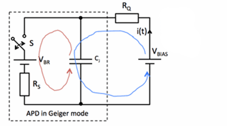
Figure 4. A simplified electrical equivalent circuit of a microcell externally biased with VBIAS.
Figure 4 shows a simplified electrical equivalent circuit of a microcell that is externally biased with VBIAS. In the absence of light and dark counts, the microcell is in Geiger mode: the switch S is open, the voltage on the junction capacitance CJ is VBIAS, and no current flows through the quenching resistor RQ or the series resistance RS. At the instant a charge carrier triggers a discharge (avalanche), the switch S closes and CJ begins to discharge through RS (shown in the figure with the red swirl) causing a voltage drop on RQ and, thus, a current through the terminals of the SiPM.
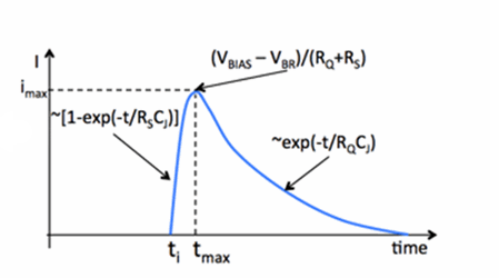
Figure 5. Graph of current pulse.
Figure 5 shows the current pulse begins at ti. The current rapidly increases until it reaches the maximum value imax = (VBIAS - VBR)/(RQ + RS) at tmax, which is on the order of ~1 ns. At tmax, the voltage on the APD drops to approximately VBR, which is not enough to sustain the discharge. Quenching occurs. The junction capacitance CJ begins recharging, causing the voltage across RQ to be decreasing and, thus, the current through the terminals of the SiPM to be also decreasing exponentially with the characteristic time τ = RQCJ. For typical values of RQ and CJ, τ ≈ 10 ns.
The amount of charge in the pulse is approximately Q = imax⋅τ. The gain is then:
Equation 1
But RQ ≫ RS, thus
Equation 2
where ΔV≡ VBIAS ‐ VBR is known as "overvoltage." The equation for the gain shows that μ varies linearly with ΔV and CJ and, somewhat surprisingly, it does not depend on RQ. The value of CJ is fixed by the specific architecture of the SiPM; thus, ΔV is the adjustable parameter that controls μ. There is no explicit dependence of μ on temperature; however, because VBR does depend on temperature, so does μ for a fixed VBIAS. To eliminate the temperature dependence of the gain, the SiPM should be operated so that ΔV is constant.
In the linear relationship between the gain and overvoltage shown by Figure 6 for three SiPMs, note that for a given ΔV, the gain increases with the size of a microcell and, thus, with CJ.
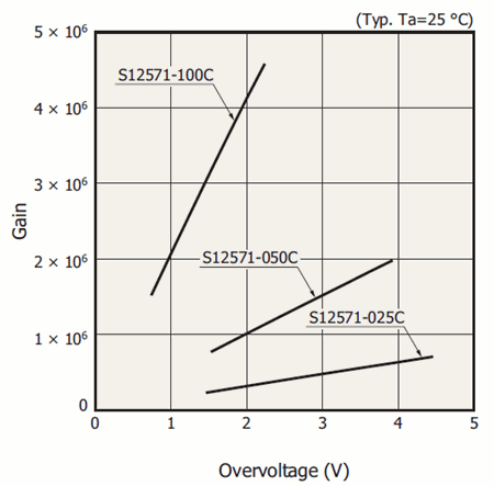
Figure 6. The linear relationship between the gain and overvoltage for three SiPMs manufactured by Hamamatsu: S12571-100C, S12571-050C, and S12571-025C.
What is the photon detection efficiency (PDE) of a SiPM?
Photon detection efficiency (ξ) is a probability that a silicon photomultiplier (SiPM) produces an output signal in response to an incident photon. It is a function of overvoltage ΔV and wavelength λ of the incident light, and can be expressed as a product ξ(ΔV,λ) = ƒ · η · PG. In the equation, ƒ is a geometrical fill factor, η quantum efficiency, and PG probability of Geiger discharge. Photon detection efficiency is a key characteristic of a SiPM; below is its more detailed discussion.
Geometrical fill factor
A SiPM is a pixelated device. In a given SiPM, all of the pixels, or microcells, are square, of the same size, and arranged in a rectangular (tiled) pattern. The total area occupied by the microcells is known as an active area. Depending on the design of a SiPM, the active areas range from 1 x 1 mm2 to 6 x 6 mm2. Because certain regions of a microcell have no photosensitivity, only some fraction of the active area is sensitive to light. This fraction is known as the geometrical fill factor. The values of ƒ range from ∼30% to ∼80%, with the larger value for the larger size of a microcell.
Quantum efficiency
This parameter is the probability that an incident photon produces a charge carrier (electron or hole) capable of triggering Geiger discharge in the avalanche section of the depletion region. The layered structure of a SiPM can be optimized through the Beers-Lambert law so that the absorption of light occurs in the depletion layer for the desired range of wavelengths. An electric field in the depletion region separates the photo-generated electron-hole pair and injects one of the charge carriers into the avalanche region. Outside of the depletion region, the electric field is weak and the photo-generated electron-hole pair is likely to recombine. The above discussion implies that η is a function of wavelength.
Probability of Geiger discharge
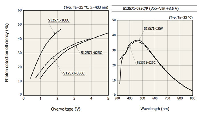
Figure 7. Samples of plots showing how ξ depends on ΔV and λ.
Once in the avalanche region, the injected charge carrier gains kinetic energy from the electric field and if the kinetic energy exceeds the ionization threshold, may be able to impact-ionize silicon atoms, thus triggering an avalanche. The likelihood of this scenario depends on three factors: 1) the strength of the electric field, which is controlled by ΔV; 2) the width of the avalanche region, which also depends on ΔV and 3) collisional cross section of charge carriers with phonons and the specific history of these interactions. If ΔV < 0, the likelihood of Geiger discharge is exceedingly small. As ΔV increases above 0, the kinetic energy of a charge carrier can be above the ionization threshold energy and, moreover, the width of the avalanche region widens, making the likelihood increasingly higher. Inelastic scattering of charge carriers with phonons increases with ΔV, which limits steeply the likelihood of Geiger discharge rising with ΔV. The figures are samples of plots showing how ξ depends on ΔV and λ.
How to measure breakdown voltage in a SiPM
The construction of a silicon photomultiplier (SiPM) consists of microcells (pixels) connected in parallel. Each microcell is a series combination of an avalanche photodiode (APD) and a quenching resistor. In a normal application, an external voltage source VBIAS biases the SiPM so that each APD operates in Geiger mode: the voltage on the APD, equal to VBIAS, is larger than its breakdown voltage, VBD. The difference VBIAS − VBD is known as overvoltage ΔV, which is one of the most important parameters affecting the operation of a SiPM. Thus, knowing the value of VBD is crucial because it determines the required value of VBIAS for the desired ΔV. VBD is the key characteristic of a SiPM.
Measuring VBD
Several techniques of measuring VBD exist. This note describes one that relies on the reverse-bias I-V characteristic. Figure 8 shows the experimental setup. The SiPM is in darkness, inside of a temperature-controlled "black box." It is reverse-biased with a voltage source VS and the picoammeter A measures the current.
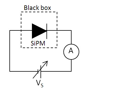
Figure 8. Diagram of experimental setup for measuring VBD inside a temperature-controlled "black box."
Figure 9 shows a possible I-V characteristic around VBD.1 For VS << VBD (not shown), the (dark) current I monotonically increases with VS. The dark current has two contributions: 1) the bulk current due to thermally generated charge carriers, primarily in the depletion region, and 2) the surface current due to defects at the Si-SiO2 interface. Both contributions increase with VS. As VS approaches VBD, the carriers generated in the bulk begin to have enough energy to impact ionize Si atoms in the avalanche section of the depletion region — an APD has a gain larger than 1. The current now increases more rapidly with each voltage step, reaching the highest rate of increase when VS = VBD. For VS > VBD, the APDs operate in Geiger mode, with the gain linearly proportional to ΔV. In addition, crosstalk and afterpulsing contribute to the net current. The current increases with the voltage but at the smaller rate than when VS was approaching VBD. However, as VS increases further, another region develops on the I-V characteristic where the current sharply increases with VS. Here, the density of charge carriers is so high that the quenching resistors cannot restore the APDs back to Geiger mode and the SiPM becomes an Ohmic device. Plotting d(log I)/dVS versus VS reveals the voltages at which the maximum rate of the current increase with voltage occurs; these voltages correspond to the peaks on this plot.
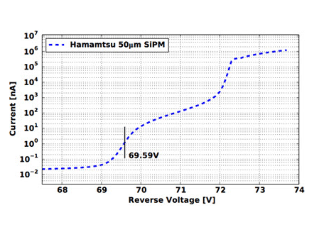
Figure 9. Plot of a possible I-V characteristic around VBD.
Figure 10 shows such a plot for the I-V characteristics listed in this scenario. The first peak (at the lower voltage) exists at VBD. This is how VBD can be measured. The precision of the measurement depends on the voltage step used while performing the sweep. A smaller step yields more accurate determination of VBD. In practice, one would first determine the approximate value of VBD with coarse voltage steps. A finer sweep around VBD would follow. Repeating the finer sweeps and averaging the results would further improve the accuracy of the measured VBD.
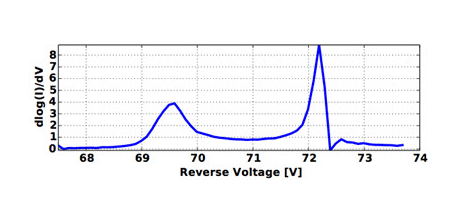
Figure 10. Plot of d(log I)/dVs versus Vs for the I-V characteristics plot in Figure 9.
S/N in a continuous wave operation of a SiPM
Analogously to a photomultiplier tube, a SiPM can operate in two distinct modes: continuous wave and photon counting. In the former, the output pulses are neither detected nor counted individually; instead, an analog output current is measured. In the latter, the individual pulses are either counted (digital photon counting) or integrated to yield the charge released in Geiger discharge (analog photon counting). The choice of the detection technique depends, among other factors, on the frequency and duration of the output pulses. If the pulses are crowded and overlapping, the continuous wave mode is appropriate. If the pulses are distinguishable, then photon counting — analog or digital — is preferable.
Continuous mode operation
If the individual output current waveforms have a significant overlap, the continuous wave operation of a SiPM is warranted. Suppose a monochromatic light with average power P illuminates the active area of a SiPM. In response, the average signal current is:
Equation 3
where μ and ξ are the gain and photon detection efficiency of the SiPM, respectively; λ is wavelength of the incident light; e is the fundamental charge; h is Planck's constant; and c is the speed of light. The total output current, Iout, is a superposition of dark current, Id, signal current, IS, and the "excess current" due to crosstalk and afterpulsing. In the first-order approximation, the excess current is (Pct + Pap)IS, where Pct and Pap are the probabilities of crosstalk and afterpulsing, respectively. Thus, Iout = Id + IS + (Pct+Pap)IS. This equation assumes that Id already includes the contributions from crosstalk and afterpulsing.
For the measured values of Iout and Id, the photo-generated current is:
Equation 4
Equating equations 3 and 4 and solving for P yields for the incident light power:
Equation 5
Signal-to-noise ratio
If IS is measured under the conditions that the measurement bandwidth is B (in Hz) and the excess noise figure is F, then the signal-to-noise ratio is given by
Equation 6
where id = √(2eμBFId) and iS = √(2eμBFIS) are expressions for the shot noise of dark current and signal current, respectively, and IS is given by Equation 4. Note that the expressions for the dark current and photocurrent shot noise contain only one power of μ because both the dark current and the photocurrent are already amplified by μ.
Excess noise figure
The excess noise figure F must be known for the above equation for S/N to be useful. The theoretical understanding of F is still lacking because numerous factors may contribute to F in a complex way. It is likely that F is a function of overvoltage, input light level, crosstalk probability, afterpulsing probability, microcell-to-microcell gain variations, and stochastic nature of the gain mechanism in a single microcell.
Optical crosstalk in a SiPM
Optical crosstalk occurs when a primary discharge (avalanche) in a microcell triggers secondary discharges in one or more adjacent microcells. The secondary discharge may be nearly simultaneous with the primary (direct or prompt crosstalk) or delayed by several 10's of ns (delayed crosstalk). Optical crosstalk is an example of a correlated noise: it can be present only if a primary discharge is present. The primary discharge can be due to 1) absorption of a photon, 2) thermal generation of a charge carrier in the multiplication region, 3) injection of a charge carrier, thermally generated outside of the avalanche region, into the avalanche region, or 4) crosstalk-induced secondary discharge becoming the primary discharge for subsequent crosstalk events. If not corrected for, crosstalk makes the output signal higher than that implied by the amount of the incident light.
Mechanism
The figure below depicts the mechanism for the prompt (P-CT), delayed (D-CT), and no (No-CT) crosstalk. The primary avalanche in the middle pixel creates three representative photons. One of them moves directly to the avalanche region of the microcell on the right and triggers a simultaneous secondary avalanche there. This is a direct or prompt crosstalk (P-CT). The other photon creates a charge carrier in the vicinity of the avalanche region of the microcell on the left. The charge carrier diffuses to the avalanche region, triggering a secondary avalanche that is delayed with respect to the primary. This is a delayed crosstalk (D-CT). The third photon leaves the SiPM; no crosstalk occurs (No-CT). The majority of photons produced by the primary discharge does not produce crosstalk.
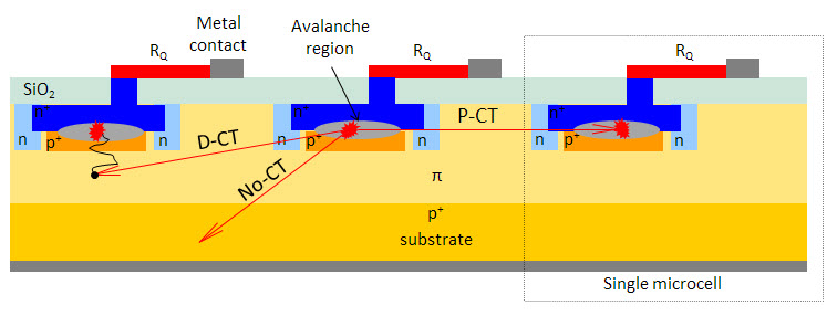
Figure 11. This diagram depicts the mechanism for the prompt (P-CT), delayed (D-CT), and no (No-CT) crosstalk. (It also shows a typical structure of a SiPM, but it does not correspond to the actual structure of the Hamamatsu product.)
Dependence
The probability of optical crosstalk depends on several factors: 1) the size of a microcell, 2) the layered architecture of a SiPM, and 3) the difference between the bias voltage and the breakdown voltage, or the overvoltage. For a given SiPM, the first two factors are fixed; therefore, the overvoltage is the parameter that primarily controls the probability. The probability increases with increasing overvoltage.
Consequences
- If a SiPM is used to measure the incident photon flux, whether it is by photon counting or continuous wave operation, crosstalk causes an appearance of a higher incident flux.
- Crosstalk is the main contributor to the excess noise figure.
- Crosstalk effectively limits the practical setting for the gain.
Measuring crosstalk probability in a SiPM
A Geiger discharge in a microcell of a SiPM emits isotropically about a few tens of photons that have enough energy to create an electron-hole pair. Most of these photons either escape the SiPM or create pairs far from the avalanche region. However, there is a finite probability that a photon creates a pair in, or close to, an avalanche region of a nearby microcell. One of the charge carriers from the pair may trigger a secondary avalanche — this avalanche is known as crosstalk. It is also possible that not only one but two, or more, photons emitted by the primary discharge trigger secondary discharges. The probability of crosstalk for a given SiPM is a function of overvoltage ΔV. This note describes a method of measuring crosstalk probability PCT.
Output waveforms
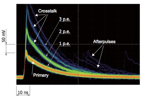
Figure 12. An oscilloscope trace with the display set to persistence mode.
In the absence of crosstalk, the output waveform resembles the one labeled 1 p.e. in the figure above. If the primary avalanche is accompanied by one secondary crosstalk discharge, the resulting waveform, labeled 2 p.e. in the figure, is a superposition of two 1 p.e. waveforms. If it is accompanied by two, a 3 p.e. waveform results, and so on. The figure is an oscilloscope trace with the display set to persistence mode. The SiPM is in darkness; the 1 p.e. waveforms are due to dark counts. The color gradient, from warmer (red) to cooler (blue), is proportional to the "density" of waveforms, that is, the frequency of occurrence. The most common events are 1 p.e., followed by 2 p.e., 3 p.e., etc. All of the waveforms that are different from 1 p.e. are due to crosstalk.
Measuring crosstalk probability
The primary waveforms (1 p.e.) are due to dark counts; whereas, 2 p.e., 3 p.e., etc. are due to crosstalk. Let N1p.e., N2p.e., N3p.e. be the number of 1 p.e., 2 p.e., 3 p.e., etc. waveforms counted within some observation time τ. Therefore, the dark count rate is (N1p.e. + N2p.e. + N3p.e. +... )/τ, whereas the probability of crosstalk is PCT = (N2p.e. + N3p.e. + N4p.e. + ...)/(N1p.e. + N2p.e. + N3p.e. + ...).
A relatively simple procedure to measure this probability is to count the number of waveforms with the setup shown in Figure 13.

Figure 13. Diagram of a simple setup to measure probability of crosstalk.
The SiPM operates in the dark. The wide-bandwidth amplifier G converts the output current signal to a voltage signal and amplifies the signal's strength. The output of the amplifier is an input to a digital counter such as Tektronix FCA3100. The counter counts a signal if its amplitude exceeds a certain user-set level (lower discrimination threshold). The experimental data consist of the number of counts per unit time as a function of threshold level. Plotting this data produces the characteristic "staircase" shown in Figure 14.
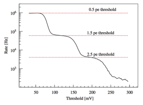
Figure 14. Plot of experimental data producing characteristic "staircase."
The vertical axis plots the count rate (frequency) and the horizontal axis the threshold level. The frequency corresponding to the top red line is due to all detectable waveforms, whereas that for the red line below the top is due to crosstalk waveforms. Referring to the first frequency as ν0.5p.e. and the other as ν1.5p.e., the probability of crosstalk is PCT = ν1.5p.e./ν0.5p.e..
References
1 Adopted from "Study of the Silicon Photomultipliers and Their Applications in Positron Emission Tomography," PhD Dissertation by Chen Xu.
About the author
Slawomir S. Piatek, PhD, is a senior university lecturer of physics at New Jersey Institute of Technology. In his role as scientific consultant at Hamamatsu Corporation, he has developed a photonics training program for engineers and is involved in popularizing SiPM as a novel photodetector by writing and lecturing about the device.
- Confirmation
-
It looks like you're in the . If this is not your location, please select the correct region or country below.
You're headed to Hamamatsu Photonics website for US (English). If you want to view an other country's site, the optimized information will be provided by selecting options below.
In order to use this website comfortably, we use cookies. For cookie details please see our cookie policy.
- Cookie Policy
-
This website or its third-party tools use cookies, which are necessary to its functioning and required to achieve the purposes illustrated in this cookie policy. By closing the cookie warning banner, scrolling the page, clicking a link or continuing to browse otherwise, you agree to the use of cookies.
Hamamatsu uses cookies in order to enhance your experience on our website and ensure that our website functions.
You can visit this page at any time to learn more about cookies, get the most up to date information on how we use cookies and manage your cookie settings. We will not use cookies for any purpose other than the ones stated, but please note that we reserve the right to update our cookies.
1. What are cookies?
For modern websites to work according to visitor’s expectations, they need to collect certain basic information about visitors. To do this, a site will create small text files which are placed on visitor’s devices (computer or mobile) - these files are known as cookies when you access a website. Cookies are used in order to make websites function and work efficiently. Cookies are uniquely assigned to each visitor and can only be read by a web server in the domain that issued the cookie to the visitor. Cookies cannot be used to run programs or deliver viruses to a visitor’s device.
Cookies do various jobs which make the visitor’s experience of the internet much smoother and more interactive. For instance, cookies are used to remember the visitor’s preferences on sites they visit often, to remember language preference and to help navigate between pages more efficiently. Much, though not all, of the data collected is anonymous, though some of it is designed to detect browsing patterns and approximate geographical location to improve the visitor experience.
Certain type of cookies may require the data subject’s consent before storing them on the computer.
2. What are the different types of cookies?
This website uses two types of cookies:
- First party cookies. For our website, the first party cookies are controlled and maintained by Hamamatsu. No other parties have access to these cookies.
- Third party cookies. These cookies are implemented by organizations outside Hamamatsu. We do not have access to the data in these cookies, but we use these cookies to improve the overall website experience.
3. How do we use cookies?
This website uses cookies for following purposes:
- Certain cookies are necessary for our website to function. These are strictly necessary cookies and are required to enable website access, support navigation or provide relevant content. These cookies direct you to the correct region or country, and support security and ecommerce. Strictly necessary cookies also enforce your privacy preferences. Without these strictly necessary cookies, much of our website will not function.
- Analytics cookies are used to track website usage. This data enables us to improve our website usability, performance and website administration. In our analytics cookies, we do not store any personal identifying information.
- Functionality cookies. These are used to recognize you when you return to our website. This enables us to personalize our content for you, greet you by name and remember your preferences (for example, your choice of language or region).
- These cookies record your visit to our website, the pages you have visited and the links you have followed. We will use this information to make our website and the advertising displayed on it more relevant to your interests. We may also share this information with third parties for this purpose.
Cookies help us help you. Through the use of cookies, we learn what is important to our visitors and we develop and enhance website content and functionality to support your experience. Much of our website can be accessed if cookies are disabled, however certain website functions may not work. And, we believe your current and future visits will be enhanced if cookies are enabled.
4. Which cookies do we use?
There are two ways to manage cookie preferences.
- You can set your cookie preferences on your device or in your browser.
- You can set your cookie preferences at the website level.
If you don’t want to receive cookies, you can modify your browser so that it notifies you when cookies are sent to it or you can refuse cookies altogether. You can also delete cookies that have already been set.
If you wish to restrict or block web browser cookies which are set on your device then you can do this through your browser settings; the Help function within your browser should tell you how. Alternatively, you may wish to visit www.aboutcookies.org, which contains comprehensive information on how to do this on a wide variety of desktop browsers.
5. What are Internet tags and how do we use them with cookies?
Occasionally, we may use internet tags (also known as action tags, single-pixel GIFs, clear GIFs, invisible GIFs and 1-by-1 GIFs) at this site and may deploy these tags/cookies through a third-party advertising partner or a web analytical service partner which may be located and store the respective information (including your IP-address) in a foreign country. These tags/cookies are placed on both online advertisements that bring users to this site and on different pages of this site. We use this technology to measure the visitors' responses to our sites and the effectiveness of our advertising campaigns (including how many times a page is opened and which information is consulted) as well as to evaluate your use of this website. The third-party partner or the web analytical service partner may be able to collect data about visitors to our and other sites because of these internet tags/cookies, may compose reports regarding the website’s activity for us and may provide further services which are related to the use of the website and the internet. They may provide such information to other parties if there is a legal requirement that they do so, or if they hire the other parties to process information on their behalf.
If you would like more information about web tags and cookies associated with on-line advertising or to opt-out of third-party collection of this information, please visit the Network Advertising Initiative website http://www.networkadvertising.org.
6. Analytics and Advertisement Cookies
We use third-party cookies (such as Google Analytics) to track visitors on our website, to get reports about how visitors use the website and to inform, optimize and serve ads based on someone's past visits to our website.
You may opt-out of Google Analytics cookies by the websites provided by Google:
https://tools.google.com/dlpage/gaoptout?hl=en
As provided in this Privacy Policy (Article 5), you can learn more about opt-out cookies by the website provided by Network Advertising Initiative:
http://www.networkadvertising.org
We inform you that in such case you will not be able to wholly use all functions of our website.
Close


