Application notes

Technical notes
Ask an engineer


Publications
United States (EN)
Select your region or country.
Silicon photomultipliers (SiPM): The ultimate photosensor?
Peter Seitz, PhD, Hamamatsu Photonics Europe
June 2, 2017
In 1946, the world's first general-purpose computer ENIAC was revealed to the astounded public. The ENIAC employed 17,478 vacuum tubes and it consumed 150 kW of electricity. Barely 20 years later, the first all-transistor desktop calculators appeared on the market, and since then, nobody in their right mind is using vacuum tubes any more to build a computer.
In photosensing, the situation is completely different. The photomultiplier tube was invented in 1934, and just six years later the first all-silicon photodiode was demonstrated in 1940. Despite the amazing progress of silicon technology since this time, millions of photomultiplier tubes (PMT) are still being sold every year. What is the reason behind this baffling fact? Why have semiconductors not completely replaced PMTs today, and are the recent developments of novel semiconductor devices such as silicon photomultipliers (SiPM) heralding the demise of the vintage PMTs?
In order to understand all this, we need to go back to basics. How can a semiconductor detect light? What limits this process, and what is the influence of the photocharge-detection electronics? In the following discussion, we will consider only three main factors, as illustrated in the simple model of Figure 1:
- The conversion of incoming photons into mobile electron-hole pairs in a semiconductor.
- The transport of photocharges to the electronic detection circuit, including the possibility of charge multiplication on the way.
- The influence of the noise of the detector electronics on the precision of the photocharge measurement.
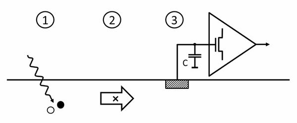
Figure 1. Simplified model of the main effects in a semiconductor photosensor
1) An incident photon with sufficient energy is converted into a mobile electron-hole pair.
2) The photogenerated mobile charges (photocharges) are transported to the electronic charge detection circuit. On their way, the avalanche effect may multiply the transported charges.
3) At the detection node, the charges to be measured are placed on the gate of the circuit's first transistor with the effective capacitance C of the detection node.
Photosensing with semiconductors and the dark noise problem
Whenever electrons are sufficiently confined in space, they are not free any more to assume any energy state; rather, their possible energy states are quantized and arranged in "allowed energy bands." In a semiconductor the situation is such that the electrons just fill up the highest occupied energy band, as illustrated in Figure 2a. At zero temperature, the electrons are all bound to their atomic cores, and there are no mobile electrons for the conduction of current. This would take an amount of energy corresponding to at least the bandgap energy Eg to lift an electron from its bound energy state to a mobile energy state; thus a mobile electron-hole pair is created.
There are two ways in which this energy can be supplied to the electrons: either by thermal excitation or by incident photons. As a consequence, a semiconductor at temperature T has always a certain concentration of mobile electron-hole pairs, which is — in a simplified case — proportional to , where k indicates Boltzmann's constant, k = 1.381 × 10⁻²³ m2 kg s-2 K-1. This situation is illustrated in Figure 2b, and it is the root cause of the famous "dark current": it is physically not possible to distinguish between a mobile electron that has been excited thermally and one that has been excited by an incident photon of sufficient energy, as illustrated in Figure 2c.
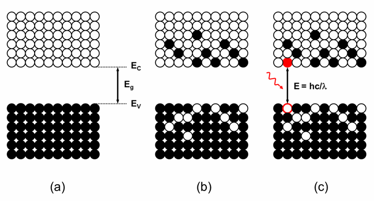
Figure 2. Energy band model of a semiconductor.
a) At zero temperature the electrons fill the available energy state just to the highest value EV (valence band). All electrons are bound to their core and no electric conductivity is possible.
b) At non-zero temperature the thermal energy is sufficient to excite some bound electrons into a mobile state in the conduction band above EC, where they can contribute to the conduction of current. This process leaves a vacancy in the valence band behind, corresponding to a mobile hole.
c) If an incident photon with wavelength λ has an energy E = hc/λ that is larger than the bandgap Eg = EC - EV, the photon is absorbed and an additional electron is excited to a mobile energy state. However, there is no way this photo-excited electron can be distinguished from a thermally excited electron.
Some readers might wonder why this discussion of semiconductors is pertinent for vacuum devices, since it is well known that PMTs employ photocathodes. As it turns out, the best photocathodes are semiconductors, and PMTs experience therefore the same effects as any other kind of semiconductor photosensor, in particular also concerning dark current.
Looking at the exponential equation given above, it is immediately clear that there are three possible approaches to reduce the dark current in a photosensor:
- Appropriate selection of the semiconductor material, so that the bandgap energy is as high as possible (for minimum dark current), but low enough that the incoming photons can still generate mobile electron-hole pairs (for sufficient quantum efficiency). As an example of how enormous the influence of the bandgap energy (and therefore the cutoff wavelength) is, consider the following three materials:
- The best silicon photosensors (for example the recent generation of Hamamatsu's Multi-Pixel Photon Counters) show a dark current density of the order of 0.05 pA/cm2 at room temperature. Silicon has a bandgap of 1.12 eV, corresponding to a cutoff wavelength of 1107 nm.
- The photocathode type S-24 is a semiconductor with a bandgap of 1.80 eV, corresponding to a cutoff wavelength of 690 nm. An S-24 based PMT has a dark current density of as low as 3 x 10⁻⁷ pA/cm2 at room temperature.
- In case infrared radiation must be sensed, a narrow-bandgap semiconductor such as InGaAs should be used. The bandgap of InGaAs is 0.73 eV, corresponding to a cutoff wavelength of 1700 nm. A good InGaAs PIN photodiode such as Hamamatsu's G11193 series has a dark current density of about 105 pA/cm2 at room temperature.
- The dark current can be substantially reduced through cooling. In the case of silicon, the dark current is halved for every reduction of the temperature by about 8 °C. As a consequence, the dark current of a silicon-based photodetector can be reduced by an order of magnitude when the temperature is lowered by about 24 °C.
- Since thermal excitation of the dark current occurs uniformly in the sensitive volume of the photosensor, one can significantly reduce the dark current by limiting the depth up to which the photosensor is still sensitive to incoming photons. This is particularly effective in PMTs, where the semiconductor photocathode is usually only a few 100 nm thick. However, this implies that the photosensor loses sensitivity and quantum efficiency. Obviously, there is a tradeoff to be made between quantum efficiency and dark current.
From the above it is very clear how the specifications of a photodetection problem influence the choice of optimum photosensor: The room-temperature dark current density of an excellent silicon-based photosensor can be around 0.05 pA/cm2, which corresponds to about 312,000 electrons/cm2/s. If the required photosensitive area in a low-light sensing problem is large (100 × 100 µm2 or more), and the typical exposure time is long (seconds), then it is simply not possible to solve the problem with a silicon-based photosensor of any type. In such cases, PMTs with larger-bandgap semiconductor photocathodes are indispensable: assuming that the photosensitive area is 1 cm2, a PMT with S-24 photocathode would have a room-temperature dark count rate of less than 2 electrons per second.
Electronic charge detection noise and the CMOS image sensor revolution
The purpose of the electronic charge detection circuit is to measure the amount of photogenerated charge Q and to produce an output signal — often a voltage — that is proportional to the charge Q. Whatever the details of the circuit are, the first stage always consists of a field effect transistor on whose gate the charge Q to be measured is placed. Due to the effective capacitance C at the gate of the transistor, the charge Q will change the gate voltage by the amount ΔV = Q/C. This voltage change influences the current through the transistor, and this current is then processed further. Unfortunately, the current through a transistor's channel is not constant; it fluctuates statistically caused by the thermal motion of the charges in the channel, the so-called Johnson noise. If one calculates back to which charge noise σQ this current noise in the channel would correspond (so-called "input-referred charge noise"), one obtains the following equation:
Equation 1
with the bandwidth B and the transistor's transconductance gm.
It is obvious what can be done to reduce this input-referred charge noise: the most effective measure is to reduce the effective input capacitance C. However, the smaller C is, the lower is also the maximum (full well) charge Qmax. In today's CMOS image sensors, a typical value of C = 1.6 fF corresponds to Qmax = CΔV = 10,000 electrons, assuming a voltage swing of ΔV = 1 V. Therefore, reducing C to sub-fF levels would significantly impair image quality due to visible Poisson noise in the pixels.
Another possibility would be to reduce the temperature T. However, lowering the temperature from 300 K to 150 K only reduces the noise by a factor of 1.414, which is disappointingly small.
At first sight, it appears that also reducing the bandwidth B is not really an option because reducing B would imply also lowering the readout rate. This was true when CCD image sensors with one or only a very few output stages were employed, with a typical bandwidth B of several 10 MHz. The significant progress brought by CMOS image sensing (CIS) technology was the implementation of a low-pass filter in each column, so that the effective bandwidth for each column is of the order of only 100 kHz. This is the real revolution brought to the image sensing domain by CIS technology. In this way, careful "bandwidth engineering" in so-called sCMOS (scientific CMOS) image sensors leads to input-referred charge noise values of a fraction of one electron at room temperature (the current world record stands at σQ ≈ 0.22 electrons r.m.s.).
It is obvious: sCMOS image sensors are capable of detecting a single photon! And given a large enough effective capacitance for the storage and measurement of the photogenerated charge, a dynamic range of 4 to 5 orders of magnitude is easily obtained!
But one thing is still elusive: while it is possible with sCMOS imagers to detect whether a photon has arrived during the exposure time, the small bandwidth of the photocharge detection electronics makes it impossible to determine the exact time when the photon has arrived. This precise timing capability is the exclusive domain of photosensors with gain.
The avalanche effect and its use in APDs and SPADs
The transistor noise equation shown above makes it very clear that there is a tradeoff in electronic circuits between the detection noise and the detection speed: only if we are ready to accept a long measurement time ("averaging") can single electrons/photons be detected. And if we want to be fast, our signal must consist of a relatively large packet of photoelectrons. As a consequence, the simultaneous detection of a single photon and its precise time of arrival necessitates a physical amplification mechanism which does not add much noise in the process. This multiplication is illustrated by the transport arrow with multiplication sign in Figure 1. Fortunately, the avalanche effect is just what is required: a single photoelectron can be converted into a packet of electrons with arbitrary size. This multiplication takes place with sub-nanosecond speed, and with a timing precision of less than 10 ps. A PMT is the perfect device for this task. The exact arrival time of each individual photon can be detected thanks to the avalanche effect in a PMT.
The solid-state equivalent to the PMT is the APD, the avalanche photodiode. Unfortunately, the choice of semiconductor materials from which good APDs can be fabricated is much more restricted than the semiconductors for good photocathodes. As a consequence, PMTs are still irreplaceable if single photons must be detected with high timing precision over large areas.
However, the avalanche effect in semiconductor devices has a property that cannot be found in PMTs. While in PMTs only electrons are involved in the multiplication process, in semiconductors electron-hole pairs are involved. Because electrons and holes are moving in opposite directions in an electric field, the avalanche can become self-sustaining in an APD when the electric field surpasses a critical value. The voltage that needs to be applied to make this happen in an APD is the breakdown voltage VBR, which is typically a few 10 V. When the voltage on an APD is below VBR, the APD is operating in the so-called linear mode, with a voltage-dependent multiplication factor. When the voltage is above VBR, the APD is operating in the Geiger mode, and it is then also called a SPAD (single photon avalanche diode). In a SPAD, the incidence of a single photon is sufficient to produce a self-sustaining avalanche. This avalanche, triggered by a single photo-generated (or thermally excited) electron, would never stop, and we therefore need to put an end to it. This is accomplished with a "quenching circuit," which consists in the simplest case of a single resistor. During the time required to suppress the avalanche, the photodetector is not responding to incident photons. For this reason, this time is called "dead time." In the case of a simple quenching resistor, the dead time is typically several 10 ns long, while active quenching circuits can reduce the dead time to 10 to 20 ns.
From SPAD to MPPC and SiPM
Although a dead time of 50 ns (in the case of a quenching resistor) does not seem much, it can still be an important impediment for the use of SPADs in case the incident photon flux shows a large dynamic range: a SPAD cannot distinguish whether one or several photons were incident during the dead time. In order to overcome this shortcoming of SPADs, so-called silicon photomultipliers (SiPM) or Multi-Pixel Photon Counters (MPPC) were invented. As illustrated in Figure 3, such an MPPC consists of several APDs, each with its own quenching resistor, connected in parallel and operated above the breakdown voltage. Whenever two photons are incident quasi-simultaneously, the current pulse at the output of the MPPC is twice as high as in the case of one incident photon. In this way it becomes possible to determine the number of incident photons by carrying out an electronic pulse-height analysis of the MPPC's output with a multi-threshold circuit, as illustrated in Figure 4. As a consequence, the MPPC is not only capable of detecting the incidence of a single photon, while determining its exact time of arrival, it is also possible to make photon flux measurements with a very high dynamic range exceeding five orders of magnitude, i.e., DR > 100 dB.
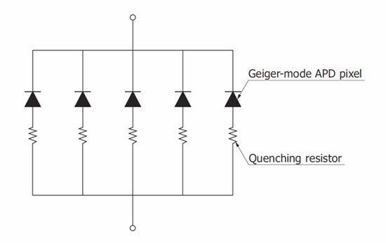
Figure 3. Construction of a SiPM (also called MPPC), consisting of the parallel operation of several SPADs (APDs operated in Geiger mode), each provided with its own quenching resistor.
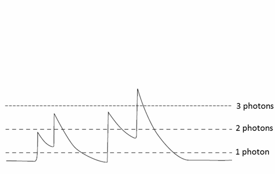
Figure 4. Typical signal of an MPPC, when several photons are impinging concurrently or shortly after each other. By exploiting the amplitude of the signal, it becomes possible to detect also the quasi-simultaneous incidence of several photons without any dead-time effects.
Of course, several MPPC devices can be arranged in a two-dimensional array, forming an MPPC image sensor. Such an MPPC imager shows ultimate single-photon sensitivity, it also provides exact time-of-arrival information, it has a high dynamic range, and the photon number information is already available in digital format. However, this almost-ideal performance comes at a price: since each MPPC pixel requires its own multi-threshold pulse-height analysis electronics, time-to-digital converter (TDC), digital counters and memory cells, all this circuitry needs substantial floor space on the silicon beneath or on the side of a pixel's SPAD array. As a consequence, a typical digital MPPC pixel can have a pitch of the order of 100 µm. Since today's most advanced CMOS image sensors exhibit a pixel pitch of about 1 µm, it follows that 10,000 (analog) CMOS pixels fit on the same area as one (digital) MPPC pixel.
Summary: the optimum photosensor for your photonic measurement problem
Finally, we are able to answer the question with which we started. Despite the amazing advances of semiconductor technology over the past 60 years, there is still no universal solid-state photosensor, and there are still applications where PMTs are simply irreplaceable.
Today, all types of photosensors — PMT, sCMOS, APD, SPAD and SiPM (MPPC) — are capable of detecting the arrival of a single photon. In cases where a large number of very small (micron-sized) pixels are required, only sCMOS technology is an option. Conversely, when it is necessary to know also the exact arrival time of an individual photon, only PMT, APD, SPAD and SiPM (MPPC) solutions are possible. If a very large dynamic range of the time-of-arrival measurement capability is required, only PMT and SiPM (MPPC) technology can provide the necessary performance. In cases where a large photosensitive area, long exposure times, accurate time-of-arrival information and a high dynamic range are needed — and strong cooling is not permitted — only PMTs with suitable photocathode materials are an option. And SiPM (MPPC) is the only possibility when image sensing with single-photon resolution, exact time-of-arrival determination, a high dynamic range, low power consumption and digital output in a single-chip solution are required.
- Confirmation
-
It looks like you're in the . If this is not your location, please select the correct region or country below.
You're headed to Hamamatsu Photonics website for US (English). If you want to view an other country's site, the optimized information will be provided by selecting options below.
In order to use this website comfortably, we use cookies. For cookie details please see our cookie policy.
- Cookie Policy
-
This website or its third-party tools use cookies, which are necessary to its functioning and required to achieve the purposes illustrated in this cookie policy. By closing the cookie warning banner, scrolling the page, clicking a link or continuing to browse otherwise, you agree to the use of cookies.
Hamamatsu uses cookies in order to enhance your experience on our website and ensure that our website functions.
You can visit this page at any time to learn more about cookies, get the most up to date information on how we use cookies and manage your cookie settings. We will not use cookies for any purpose other than the ones stated, but please note that we reserve the right to update our cookies.
1. What are cookies?
For modern websites to work according to visitor’s expectations, they need to collect certain basic information about visitors. To do this, a site will create small text files which are placed on visitor’s devices (computer or mobile) - these files are known as cookies when you access a website. Cookies are used in order to make websites function and work efficiently. Cookies are uniquely assigned to each visitor and can only be read by a web server in the domain that issued the cookie to the visitor. Cookies cannot be used to run programs or deliver viruses to a visitor’s device.
Cookies do various jobs which make the visitor’s experience of the internet much smoother and more interactive. For instance, cookies are used to remember the visitor’s preferences on sites they visit often, to remember language preference and to help navigate between pages more efficiently. Much, though not all, of the data collected is anonymous, though some of it is designed to detect browsing patterns and approximate geographical location to improve the visitor experience.
Certain type of cookies may require the data subject’s consent before storing them on the computer.
2. What are the different types of cookies?
This website uses two types of cookies:
- First party cookies. For our website, the first party cookies are controlled and maintained by Hamamatsu. No other parties have access to these cookies.
- Third party cookies. These cookies are implemented by organizations outside Hamamatsu. We do not have access to the data in these cookies, but we use these cookies to improve the overall website experience.
3. How do we use cookies?
This website uses cookies for following purposes:
- Certain cookies are necessary for our website to function. These are strictly necessary cookies and are required to enable website access, support navigation or provide relevant content. These cookies direct you to the correct region or country, and support security and ecommerce. Strictly necessary cookies also enforce your privacy preferences. Without these strictly necessary cookies, much of our website will not function.
- Analytics cookies are used to track website usage. This data enables us to improve our website usability, performance and website administration. In our analytics cookies, we do not store any personal identifying information.
- Functionality cookies. These are used to recognize you when you return to our website. This enables us to personalize our content for you, greet you by name and remember your preferences (for example, your choice of language or region).
- These cookies record your visit to our website, the pages you have visited and the links you have followed. We will use this information to make our website and the advertising displayed on it more relevant to your interests. We may also share this information with third parties for this purpose.
Cookies help us help you. Through the use of cookies, we learn what is important to our visitors and we develop and enhance website content and functionality to support your experience. Much of our website can be accessed if cookies are disabled, however certain website functions may not work. And, we believe your current and future visits will be enhanced if cookies are enabled.
4. Which cookies do we use?
There are two ways to manage cookie preferences.
- You can set your cookie preferences on your device or in your browser.
- You can set your cookie preferences at the website level.
If you don’t want to receive cookies, you can modify your browser so that it notifies you when cookies are sent to it or you can refuse cookies altogether. You can also delete cookies that have already been set.
If you wish to restrict or block web browser cookies which are set on your device then you can do this through your browser settings; the Help function within your browser should tell you how. Alternatively, you may wish to visit www.aboutcookies.org, which contains comprehensive information on how to do this on a wide variety of desktop browsers.
5. What are Internet tags and how do we use them with cookies?
Occasionally, we may use internet tags (also known as action tags, single-pixel GIFs, clear GIFs, invisible GIFs and 1-by-1 GIFs) at this site and may deploy these tags/cookies through a third-party advertising partner or a web analytical service partner which may be located and store the respective information (including your IP-address) in a foreign country. These tags/cookies are placed on both online advertisements that bring users to this site and on different pages of this site. We use this technology to measure the visitors' responses to our sites and the effectiveness of our advertising campaigns (including how many times a page is opened and which information is consulted) as well as to evaluate your use of this website. The third-party partner or the web analytical service partner may be able to collect data about visitors to our and other sites because of these internet tags/cookies, may compose reports regarding the website’s activity for us and may provide further services which are related to the use of the website and the internet. They may provide such information to other parties if there is a legal requirement that they do so, or if they hire the other parties to process information on their behalf.
If you would like more information about web tags and cookies associated with on-line advertising or to opt-out of third-party collection of this information, please visit the Network Advertising Initiative website http://www.networkadvertising.org.
6. Analytics and Advertisement Cookies
We use third-party cookies (such as Google Analytics) to track visitors on our website, to get reports about how visitors use the website and to inform, optimize and serve ads based on someone's past visits to our website.
You may opt-out of Google Analytics cookies by the websites provided by Google:
https://tools.google.com/dlpage/gaoptout?hl=en
As provided in this Privacy Policy (Article 5), you can learn more about opt-out cookies by the website provided by Network Advertising Initiative:
http://www.networkadvertising.org
We inform you that in such case you will not be able to wholly use all functions of our website.
Close