Application notes

Technical notes
Ask an engineer


Publications
United States (EN)
Select your region or country.
How does temperature affect the performance of an SiPM?
Slawomir Piatek, PhD, Hamamatsu Corporation & New Jersey Institute of Technology
January 4, 2017
Introduction
A silicon photomultiplier (SiPM) is a solid-state device capable of detecting single photons due to its very high internal gain (106 – 107). A SiPM is a rectangular matrix of square microcells (10 – 100 µm on the side) numbering from several hundreds to several tens of thousands depending on the model. Each microcell is a series combination of an avalanche photodiode (APD) operating in Geiger mode and a quenching resistor RQ. All of the microcells are identical and connected in parallel. In a typical operation, a SiPM is reversed biased with the voltage VBIAS that is a few volts above the breakdown voltage VBD of the APDs. The difference VBIAS - VBD is known as the overvoltage ΔV. Overvoltage is one of the key parameters controlling the operation and opto-electronic characteristics of the detector. In response to light or internally generated charge carriers, a SiPM acts like a current source — the output is a superposition of current pulses produced by the activated, or fired, microcells.
Temperature plays a significant role in the operation of all solid-state devices, including SiPMs. Its varied effects include influencing the concentration of charge carriers in doped and intrinsic semiconductors, thus affecting their resistivity; controlling the phonon spectrum, thus affecting electron-phonon and hole-phonon interactions; and setting the rate of thermal generation of charge carriers, thus affecting the amount of output dark current. This technical note examines and summarizes the present understanding of how changing temperature affects the key opto-electronic characteristics of a SiPM. It relies on published results in peer-reviewed articles and is organized into semi-autonomous sections, each discussing a particular characteristic.
Quenching resistance
RQ passively terminates Geiger discharge in a microcell. Its value affects the amplitude of a single photoelectron current pulse (often referred to as 1 p.e. pulse or waveform) and, together with the junction capacitance CJ, the recovery time. If the value of RQ were to fall below a certain threshold, quenching would not have occurred, leaving the microcell in the state of a permanent Geiger discharge and insensitivity to light. The value of RQ can be deduced from the forward-bias I-V characteristic. As the bias increases, the current eventually becomes linearly proportional to the applied voltage because, as the resistance of the depletion region in the APDs approaches zero, only RQs limit the current. Consequently, the slope of the linear section equals N/RQ, where N is the total number of microcells. Fitting for the slope and knowing N gives RQ. I-V characteristics obtained at different temperatures yield information on how RQ varies with T.
Recently, Otte et al. (2016) has performed a comprehensive study of SiPMs from three different manufacturers. Among the many tests, temperature effects within the range –40 °C to +40 °C are prominent. The left panel of Figure 1 shows I-V characteristics for the Hamamatsu S13360-3050CS SiPM, while the right panel shows how RQ varies with T. The values of RQ come from linear fits depicted as red lines in the I-V characteristics (left panel).
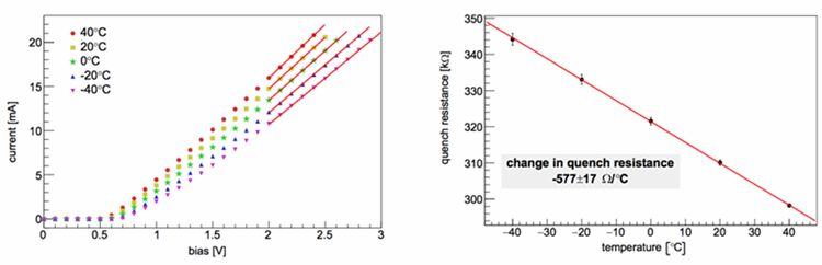
Figure 1. Forward bias I-V characteristics at different temperatures (left panel) and the corresponding values of RQ versus T (right panel). Both panels are from Otte et al. (2016).
A straight line with negative slope is a good fit to the RQ versus T data. The implied relative change of RQ with T is about 0.2% per degree Celsius. The negative temperature coefficient implies that RQ is made from a semiconductor material. Dinu et al. (2015) uses a different approach to measure RQ. The study finds that the junction capacitance of the investigated SiPMs does not vary with T, therefore, the recovery time of the output current pulses at different temperatures is only affected by RQ(T). Figure 2 depicts RQ versus T for two Hamamatsu SiPMs for the temperature range from -175 °C to +55 °C. Note that for the wider range of temperatures, the relationship is no longer linear. Instead, as expected from thermal properties of semiconductors, RQ is well fit by , where a, b and c are adjustable coefficients. The solid lines in Figure 2 are the best fits.
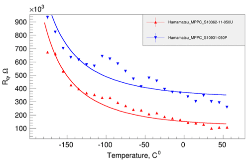
Figure 2. Quenching resistance versus temperature for two Hamamatsu SiPMs. The figure is from Dinu et al. (2015).
Breakdown voltage
Impact ionization of silicon atoms in the avalanche (or high-field) section of the depletion region is the gain mechanism in the constituent APDs of a SiPM. Here, a charge carrier (an electron or a hole) gains energy from the electric field, collides with a silicon atom ionizing it and, thus, creating an electron-hole pair. The probability of impact ionization depends on the strength of the electric field and on temperature. As temperature increases, scattering of charge carriers from the crystal lattice becomes more likely resulting in the net loss of carrier’s energy hindering impact ionization. This can be succinctly stated that the electron and hole ionization rates, α and β, are functions of temperature, both decreasing with T. To compensate the lower ionization rates, the electric field has to be strengthened by increasing the reverse bias. One expects, therefore, that the breakdown voltage VBD is a function of temperature.
Reverse-bias I-V characteristics at different temperatures can be used to determine VBD(T). The plot of versus V shows a clearly delineated peak around VBD with the maximum corresponding to V = VBD. The left panel of Figure 3 shows a family of such plots for different temperatures, while the right panel depicts the corresponding plot of VBD versus T. Both figures are for Hamamatsu S13360-3050CS SiPM and are taken from Otte et al. (2016). The figures imply that within the temperature range of the experiments, VBD increases linearly with T at the rate of about 54 mV/°C — a significant change. Other studies, for example Dinu et al. (2016) and Ferri et al. (2014), also find a linear relationship between VBD and T for a similar temperature range.
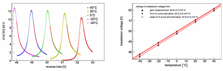
Figure 3. (Left panel) Determination of VBD from reverse-bias I-V characteristic. The derivative of the natural log of the current with respect to the applied reverse voltage has a maximum at VBD. (Right panel) The resulting relationship between VBD and T. Both figures are from Otte et al. (2016).
In another study, Collazuol et al. (2011) uses I-V characteristics to determine VBD for a much wider temperature range (50 K < T < 320 K, or -223 °C < T < 47 °C). Figure 4 shows that for any given small range of temperatures the relationship is approximately linear but over a wider range, it deviates from linearity albeit consistent with theoretical calculation (see, for example, Crowell & Sze (1966)).
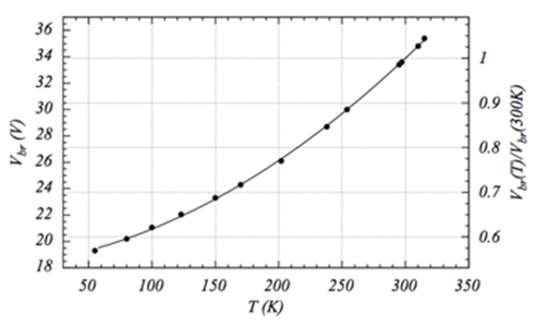
Figure 4. Breakdown voltage versus temperature for a 1 × 1 mm2 FBK-IRST SiPM type T6-V1-PD with 625 40 × 40 µm2 microcells. The figure is from Collazuol et al. (2011).
The gain µ of a SiPM equals the number of electrons that contribute to the 1 p.e. output current pulse i(t). Therefore,
Equation 1
where CJ is the junction capacitance of a single APD and e is the elementary charge. Stability of the gain under changing ambient temperature is a common requirement in practical applications. This can be accomplished by adjusting VBIAS to compensate changes of VBD and, potentially, CJ with T.
Gain and junction capacitance
As discussed above, the gain of a SiPM can be measured by integrating 1 p.e. waveforms. Doing so as a function of VBIAS and for different temperatures offers another method of determining VBD and a way of finding how CJ depends on T. The left panel of Figure 5 shows plots of µ versus VBIAS at several temperatures, while the right panel shows the corresponding plot of CJ versus T for Hamamatsu S13360-3050CS SiPM. Both figures are from Otte et al. (2016). For a given temperature, the plot of µ versus VBIAS is well fit by a straight line, implying no dependence of CJ on VBIAS. The value of VBD equals VBIAS when µ = 1, which is essentially the X intercept. The slope equals CJ/e, allowing an easy determination of CJ. The right panel of Figure 5 shows that CJ has a statistically weak dependence on T for this particular SiPM; however, other SiPMs in the study have a more significant dependence, as illustrated in Figure 6 for SensL J-series 30035 SiPM. The straight lines at different temperatures are parallel to each other implying that µ is independent of T provided that ∆V remains the same.
Click here to read more about the effects of temperature on the gain of an SiPM.
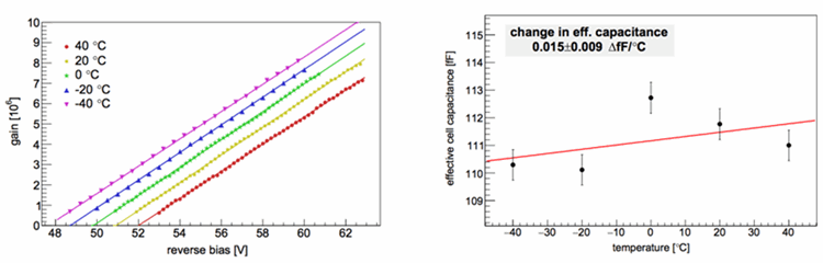
Figure 5. (Left panel) Gain versus bias voltage for several temperatures and (right panel) junction capacitance versus temperature for Hamamatsu S13360-3050CS SiPM. Both figures are from Otte et al. (2016).
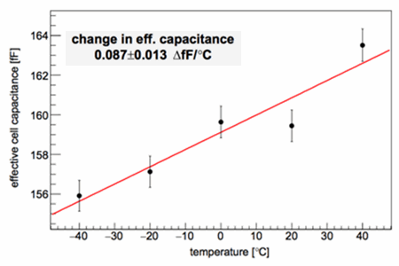
Figure 6. Junction capacitance versus temperature for SensL J-series 30035 SiPM. The figure is from Otte et al. (2016).
Signal shape
The shape of the output current pulse depends on the values of RQ and CJ (and also on the bandwidth of the detection system and load resistance). Since RQ does and CJ may vary with T, the shape too will be a function of T, as illustrated in Figure 7 (adapted from Dinu et al. 2015). The figure shows that a higher T makes a SiPM "faster" (shorter recovery time), which is highly desirable in some applications. However, the tradeoff is an increase in dark counts whose consequence is a higher minimum detectable power, or lower sensitivity.
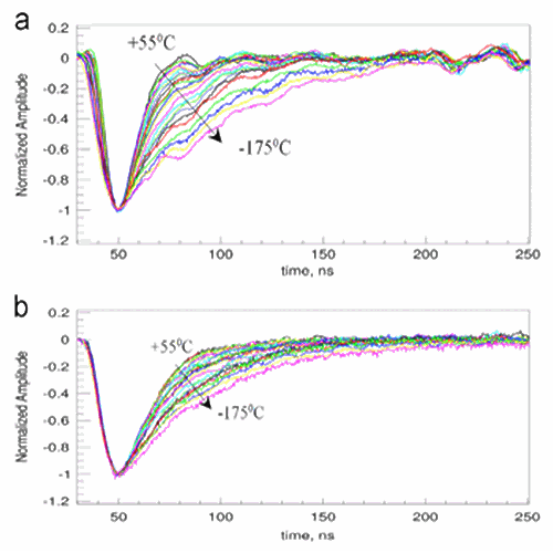
Figure 7. Normalized output averaged signals at different temperatures for (top panel) 1 × 1 mm2 and (bottom panel) 3 × 3 mm2 Hamamatsu SiPMs. The bandwidth of the detection system is 20 MHz. The figure is from Dinu et al. (2015).
Dark counts
A thermally generated (or due to quantum tunneling) charge carrier may enter (or be generated where) the high field region of an APD and trigger Geiger discharge. This possibility is known as a dark count. It results in an output that is indistinguishable from that resulting from absorption of a photon. Counting the number of the output waveforms with amplitude greater than one half of that for 1 p.e. waveform in a time interval τ gives the rate in Hertz (counted number divided by τ). The rate is a function of ΔV and T, as shown in the left panel of Figure 8. Note that the abscissa is actually the relative overvoltage:
Equation 2
The right panel shows how the rate changes with T relative to the rate at 40 °C for a fixed value of ΔVr. The rate doubles every 5.3 °C for this particular SiPM.
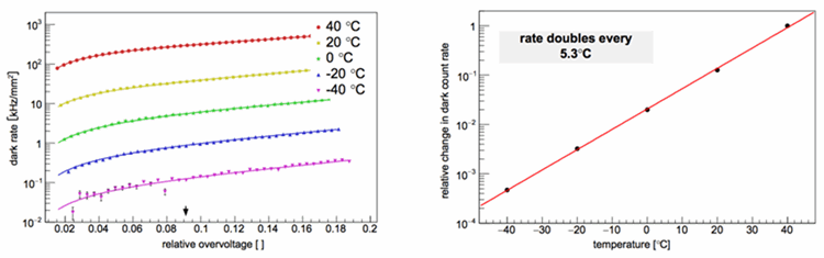
Figure 8. (Left panel) Dark count rate versus relative overvoltage for several temperatures and (right panel) relative change in dark count rate versus temperature. The figures are for Hamamatsu S13360-3050CS SiPM and adopted from Otte et al. (2016).
Noteworthy is a measurement of dark count rate as a function of T for a fixed overvoltage (1.5 V) by Collazuol et al. (2011), shown in Figure 9. The wider temperature range allowed the study to identify distinct sources of dark counts. Shockley-Read-Hall generation enhanced by trap-assisted tunneling is mostly responsible for dark counts in the region labeled a), whereas band-to-band tunneling dominates the region b). The study notes that region c) is still under investigation.
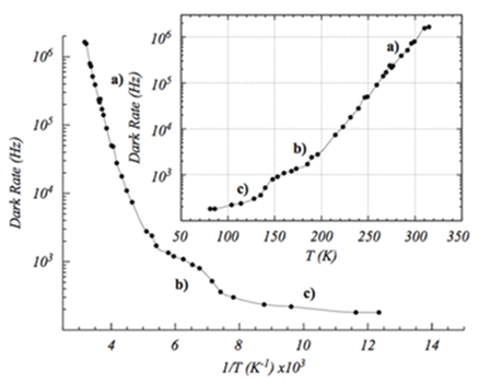
Figure 9. Dark count rate versus temperature for the same SiPM as in Figure 4. The figure is from Collazuol et al. (2011).
Optical crosstalk
Optical crosstalk is a type of correlated noise ubiquitous in SiPMs. It comes in two types: direct and delayed. When a microcell undergoes Geiger discharge, it emits about 2.9 x 10⁻⁵ photons per electron that can be reabsorbed by silicon (Lacaita et al. 1993). The total number of emitted photons is , or about 29 for µ = 106. A direct crosstalk occurs when a photon from the primary discharge moves either directly, or after a reflection, to the avalanche region of a neighboring microcell and triggers there a secondary discharge. The two resulting current pulses are nearly simultaneous producing a 2 p.e. output waveform. However, if the emitted photon is absorbed outside of the avalanche region but within the depletion region, one of the charge carriers can drift into the avalanche region and triggers a secondary discharge. The two resulting current pulses are spaced chronologically by the drift time. This is delayed crosstalk, which can resemble afterpulsing (discussed in the next section). The following discussion applies only to direct crosstalk.
The probability of optical crosstalk PCT is expected to increase with ΔV because the number of the emitted photons is linearly proportional to ΔV and because the probability of Geiger discharge PG increases with ΔV. The dependence of PCT on T for a fixed ΔV will be mostly determined by the dependence CJ with T (since CJ affects the gain and, therefore, the number of emitted photons). Figure 10 is a plot of PCT as a function of ΔVr at several temperatures for Hamamatsu S13360-3050CS SiPM. For a given ΔVr, there is only a weak dependence of PCT on T, reflecting a weak trend seen in Figure 5. In contrast, Collazuol et al. (2011) finds no evidence that PCT depends on T, which is possible if CJ of the investigated SiPM is independent of T.
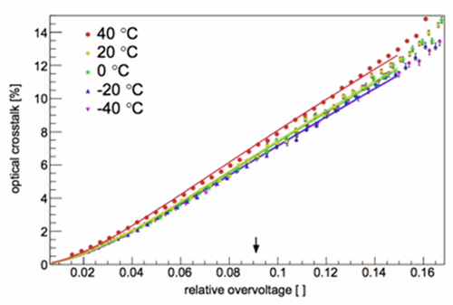
Figure 10. Probability of direct optical crosstalk as a function of relative overvoltage at several temperatures. The figure is from Otte et al. (2016).
Afterpulsing and delayed crosstalk
Impurities in silicon and crystal lattice defects can act as charge traps. A trap can capture a charge carrier created during an avalanche and then release it at a later time. If the release occurs during the recovery, the number of electrons produced in the afterpulse is less than µ and the resulting afterpulse waveform partly overlaps in time the primary; the output is their superposition. In contrast, if a trap releases charge after the complete recovery, the resulting afterpulse waveform does not overlap the primary and it is indistinguishable in shape from a 1 p.e. waveform.
Delayed crosstalk has a somewhat different signature. Here, the secondary waveform has the same amount of charge as the primary. If the drift time is less than the recovery time, the output consists of a superposition of two 1 p.e. waveforms, whereas if it is longer, two separate 1 p.e. waveforms result. The characteristic times of afterpulsing and delayed crosstalk are expected to be different because the physical processes governing them are different. Therefore, one can estimate their rates, or probabilities, from a histogram of time differences between consecutive pulses (for more details of this rather difficult measurement see Otte et al. (2016)).
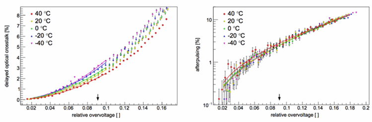
Figure 11. Plots of probability of optical crosstalk (left panel) and afterpulsing (right panel) versus relative overvoltage at several temperatures for Hamamatsu S13360-3050CS SiPM. Both plots are from Otte et al. (2016).
The plot in the left panel of Figure 11 shows how the probability of delayed optical crosstalk depends on relative overvoltage at several temperatures. As expected, the probability increases with ΔVr, though for a nominal ΔVr (marked with an arrow), it amounts to only about 2%. For fixed ΔVr, the probability increases with decreasing T (surprisingly, other SiPMs in the study show the opposite effect). The plot of afterpulsing probability as a function of ΔVr, shown in the right panel of Figure 11, does not exhibit any significant dependence on T. This is surprising because the trapping time constant is known to decrease exponentially with T, therefore, afterpulsing probability should decline with T. The probabilities of afterpulsing for the other two SiPMs investigated in the study show the opposite dependence with T. These surprising and contradictory results may have to be clarified with additional future testing. Otte et al. (2016) does note that the afterpulsing data may have been contaminated with delayed crosstalk.
Photon detection efficiency
Photon detection efficiency (PDE) is a probability that a SiPM produces an output signal in response to an incident photon. PDE is defined as a product of a geometrical fill factor, quantum efficiency (QE), and probability of Geiger discharge PG. PDE is expected to depend strongly on ΔV (through PG) and may show some dependence on T. The reasons for the latter are: 1. The band gap energy is a function of temperature, causing QE = QE(T) especially for the wavelengths close to the threshold wavelength; 2. Carrier mobility increases with T, thus PG may increase with T for fixed overvoltage; 3. Free carrier concentration depends on T, thus affecting all of the parameters that depend on the concentrations. There is very little reliable research investigating how T affects PDE. Near room temperatures, the effect is likely to be negligible but for a wider range, this may not be so, as indicated by Figure 12 from Collazuol et al. (2011). As noted by the study, more work is needed to fully understand PDE(T).
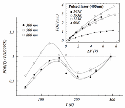
Figure 12. Normalized photon detection efficiency as a function of temperature for an overvoltage of 2V and three wavelengths (300 nm, 500 nm, and 800 nm) for 1 × 1 mm2 FBK-IRST SiPM type T6-V1-PD. The insert shows PDE as a function of overvoltage at four different temperatures.
Conclusions
Changing temperature can have a significant impact on the operation of a SiPM. Two strong dependencies on T are the value of the breakdown voltage and the dark count rate. For a stable gain, it is necessary that the ambient temperature is constant or that VBIAS is adjusted to keep the overvoltage fixed. The latter requires using a temperature-compensation circuitry. Higher dark count rate increases the minimum detectable power. In low-light applications, it may be necessary to cool the SiPM to increase its sensitivity.
References
- G. Collazuol, et al., Nuclear Instruments and Methods in Physics Research Section A 628 (2011) 389.
- Crowell, C. R., & Sze, S. M., Appl. Phys. Lett. 9 (1966) 242
- Dinu, N., Nagai, A., & Para, A. "Studies of MPPC detectors down to cryogenic temperatures," Nuclear Inst. And Methods in Physics Research, A, 787, (2015), 275-279
- Dinu, N., Nagai, A., & Para, A. "Breakdown voltage and triggering probability of SiPM from IV curves at different temperatures," Nuclear Inst. And Methods in Physics Research, A, 2016, in press
- Ferri, A., Acerbi, F., Gola, G., Paternoster, C, Piemonte, C, & Zorzi, N. "A comprehensive study of temperature stability of Silicon Photomultiplier," JINST, 2014
- A. Lacaita, M. Ghioni, F. Zappa, G. Ripamonti, S. Cova, Nuclear Instruments and Methods in Physics Research Section A: Accelerators, Spectrometers, Detectors and Associated Equipment 326 (1993) 290.
- Otte, A. N, Garcia, D., Nguyen, T., Purushotham, D. "Characterization of Three High Efficiency and Blue Sensitive Silicon Photomultipliers," Nuclear Inst. And Methods in Physics Research, A, 2016, in press.
- Piatek, S., "Effects of temperature on the gain of a SiPM," www.hamamatsu.com, published December 2016.
- Confirmation
-
It looks like you're in the . If this is not your location, please select the correct region or country below.
You're headed to Hamamatsu Photonics website for US (English). If you want to view an other country's site, the optimized information will be provided by selecting options below.
In order to use this website comfortably, we use cookies. For cookie details please see our cookie policy.
- Cookie Policy
-
This website or its third-party tools use cookies, which are necessary to its functioning and required to achieve the purposes illustrated in this cookie policy. By closing the cookie warning banner, scrolling the page, clicking a link or continuing to browse otherwise, you agree to the use of cookies.
Hamamatsu uses cookies in order to enhance your experience on our website and ensure that our website functions.
You can visit this page at any time to learn more about cookies, get the most up to date information on how we use cookies and manage your cookie settings. We will not use cookies for any purpose other than the ones stated, but please note that we reserve the right to update our cookies.
1. What are cookies?
For modern websites to work according to visitor’s expectations, they need to collect certain basic information about visitors. To do this, a site will create small text files which are placed on visitor’s devices (computer or mobile) - these files are known as cookies when you access a website. Cookies are used in order to make websites function and work efficiently. Cookies are uniquely assigned to each visitor and can only be read by a web server in the domain that issued the cookie to the visitor. Cookies cannot be used to run programs or deliver viruses to a visitor’s device.
Cookies do various jobs which make the visitor’s experience of the internet much smoother and more interactive. For instance, cookies are used to remember the visitor’s preferences on sites they visit often, to remember language preference and to help navigate between pages more efficiently. Much, though not all, of the data collected is anonymous, though some of it is designed to detect browsing patterns and approximate geographical location to improve the visitor experience.
Certain type of cookies may require the data subject’s consent before storing them on the computer.
2. What are the different types of cookies?
This website uses two types of cookies:
- First party cookies. For our website, the first party cookies are controlled and maintained by Hamamatsu. No other parties have access to these cookies.
- Third party cookies. These cookies are implemented by organizations outside Hamamatsu. We do not have access to the data in these cookies, but we use these cookies to improve the overall website experience.
3. How do we use cookies?
This website uses cookies for following purposes:
- Certain cookies are necessary for our website to function. These are strictly necessary cookies and are required to enable website access, support navigation or provide relevant content. These cookies direct you to the correct region or country, and support security and ecommerce. Strictly necessary cookies also enforce your privacy preferences. Without these strictly necessary cookies, much of our website will not function.
- Analytics cookies are used to track website usage. This data enables us to improve our website usability, performance and website administration. In our analytics cookies, we do not store any personal identifying information.
- Functionality cookies. These are used to recognize you when you return to our website. This enables us to personalize our content for you, greet you by name and remember your preferences (for example, your choice of language or region).
- These cookies record your visit to our website, the pages you have visited and the links you have followed. We will use this information to make our website and the advertising displayed on it more relevant to your interests. We may also share this information with third parties for this purpose.
Cookies help us help you. Through the use of cookies, we learn what is important to our visitors and we develop and enhance website content and functionality to support your experience. Much of our website can be accessed if cookies are disabled, however certain website functions may not work. And, we believe your current and future visits will be enhanced if cookies are enabled.
4. Which cookies do we use?
There are two ways to manage cookie preferences.
- You can set your cookie preferences on your device or in your browser.
- You can set your cookie preferences at the website level.
If you don’t want to receive cookies, you can modify your browser so that it notifies you when cookies are sent to it or you can refuse cookies altogether. You can also delete cookies that have already been set.
If you wish to restrict or block web browser cookies which are set on your device then you can do this through your browser settings; the Help function within your browser should tell you how. Alternatively, you may wish to visit www.aboutcookies.org, which contains comprehensive information on how to do this on a wide variety of desktop browsers.
5. What are Internet tags and how do we use them with cookies?
Occasionally, we may use internet tags (also known as action tags, single-pixel GIFs, clear GIFs, invisible GIFs and 1-by-1 GIFs) at this site and may deploy these tags/cookies through a third-party advertising partner or a web analytical service partner which may be located and store the respective information (including your IP-address) in a foreign country. These tags/cookies are placed on both online advertisements that bring users to this site and on different pages of this site. We use this technology to measure the visitors' responses to our sites and the effectiveness of our advertising campaigns (including how many times a page is opened and which information is consulted) as well as to evaluate your use of this website. The third-party partner or the web analytical service partner may be able to collect data about visitors to our and other sites because of these internet tags/cookies, may compose reports regarding the website’s activity for us and may provide further services which are related to the use of the website and the internet. They may provide such information to other parties if there is a legal requirement that they do so, or if they hire the other parties to process information on their behalf.
If you would like more information about web tags and cookies associated with on-line advertising or to opt-out of third-party collection of this information, please visit the Network Advertising Initiative website http://www.networkadvertising.org.
6. Analytics and Advertisement Cookies
We use third-party cookies (such as Google Analytics) to track visitors on our website, to get reports about how visitors use the website and to inform, optimize and serve ads based on someone's past visits to our website.
You may opt-out of Google Analytics cookies by the websites provided by Google:
https://tools.google.com/dlpage/gaoptout?hl=en
As provided in this Privacy Policy (Article 5), you can learn more about opt-out cookies by the website provided by Network Advertising Initiative:
http://www.networkadvertising.org
We inform you that in such case you will not be able to wholly use all functions of our website.
Close