Application notes


Technical notes
Ask an engineer


Publications
United States (EN)
Select your region or country.
The WITS$ guide to selecting a photodetector
Earl Hergert, Hamamatsu Corporation
Slawomir Piatek, PhD, Hamamatsu Corporation & New Jersey Institute of Technology
May 9, 2017
An overview of photodetector types
Photomultiplier tubes (PMT)
Photodiodes (PD)
Avalanche photodiodes (APD)
Silicon photomultipliers (SiPM)
Selecting a photodetector using the WITS$ approach
Selection based on wavelength
Selection based on intensity
Selection based on temporal characteristic of incident light
Selection based on spatial characteristic of incident light
Selection based on price
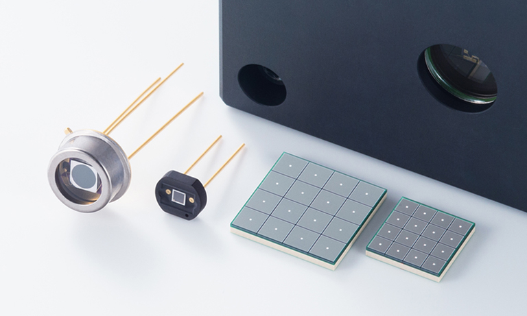
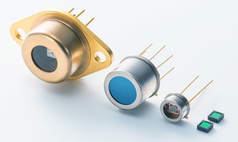
Products referenced in this article
Notes
The process of selecting an appropriate photodetector among a photomultiplier tube, photodiode, avalanche photodiode, and silicon photomultiplier may seem taxing and confusing. It involves technical tradeoffs and compromises, calculations of signal and noise, and, sometimes, budgetary considerations. The purpose of this article is to provide a qualitative and quantitative guidance to this process based on the WITS$ approach, and to illustrate it with several case studies.
Light is a versatile probe for investigating physical and chemical processes in nature. A system under investigation may infuse information about itself into the light it emits or reflects. Electrical signal is an effective medium for processing, transporting, and storing information; the role of a photodetector is to convert information propagating in the form of light into electrical signal with a minimal loss of information quality. Information carried by light may be encoded in any combination of light's four basic attributes: spectral composition (W), intensity (I), and temporal (T) and spatial (S) characteristics. The choice of the appropriate photodetector will be contingent on its performance with regard to these four aspects of light and, in addition, cost ($). The ratio of the signal and noise (S/N) at the output of a photodetector is the measure of the detector's performance and the figure of merit when choosing from an available pool of detectors. This guide is for a set of four point detectors: photomultiplier tube (PMT), photodiode (PD), avalanche photodiode (APD), and silicon photomultiplier (SiPM). What follows is their brief description.
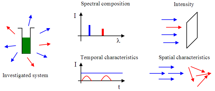
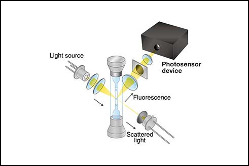
Figure 1. Light from the system under investigation may contain information about the system in the form of spectral composition, intensity (light power transferred per unit area), temporal characteristics (constant intensity, pulses, exponential decay, etc.), and spatial characteristics (directional or collimated light vs. diffuse light).
An overview of photodetector types
The following four sections describe the four photodetectors, emphasizing their typical physical, optoelectronic, and operational characteristics. Table 1 compares them; the text below discusses the entries in greater detail.
| Characteristic | PMT | PD | APD | SiPM |
| Spectral coverage [nm] | 115-1,700 | 190-13,000 | 190-1,700 | 320-900 |
| Peak QE (η) [%] | < 40 | < 90 | < 90 | < 40 (PDE) |
| Active area [mm2] | < 12,000 | < 100 | < 100 | < 10 |
| Gain (μ) | 105-106 | 1 | < 100 | 105-106 |
| NEP [W/√Hz] | > 2x10-17 | > 6x10-16 | > 1x10-15 | > 6x10-16 |
| Rise time [ns] | > 0.15 | > 0.23 | > 0.35 | > 1 |
| Bandwidth [Hz] | < 2x10⁹ | < 1.5x10⁹ | < 1x10⁹ | NA |
| Time jitter [ns] | > 0.05 | NA | > 0.2 | > 0.2 |
Photomultiplier tubes (PMT)
A PMT, depicted in Figure 2, is a vacuum tube that has the following components: a light-sensitive cathode (photocathode) where the conversion of light signal to electrical signal occurs through the process of extrinsic photoelectric effect; a sequence of dynodes (electron multipliers) where the electrical signal is amplified through the process of secondary electron emission; and an anode where the signal is received and transferred to outside detection electronics. To operate a PMT, a high voltage (around 1000 V) must be applied to it; the internal gain μ of a PMT depends on this voltage and can be on the order of 105 - 106. From the electrical standpoint, a PMT is essentially a current source in parallel with a capacitor. The output current depends on the intensity and temporal characteristics of the incident light. The capacitor represents the capacitance between the anode and the dynodes (terminal capacitance). In a typical application, a load resistor or transimpedance amplifier converts the output signal current to voltage. A PMT is capable of detecting individual photons.
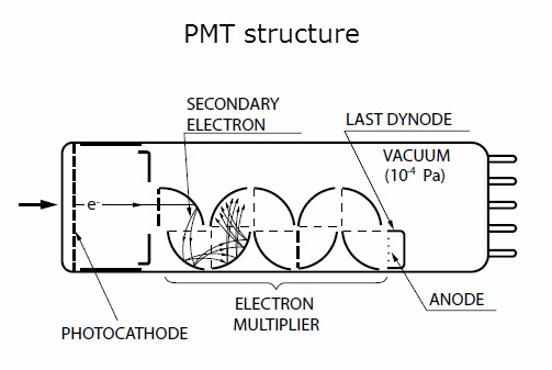
Figure 2. Structure of a photomultiplier tube (head-on type).
Hamamatsu manufactures a wide variety of PMTs. They differ in physical size, dynode structure, spectral responsivity, maximum gain, amount of dark current, time characteristics, magnetic immunity, ruggedness, and more. The multeity of designs allows a selection where a particular feature is critical (e.g., magnetic immunity, ruggedness, or time jitter).
Photodiodes (PD)
A photodiode, illustrated in Figure 3, is a solid-state device with a p-n junction. The conversion of light energy to electricity (current) occurs in the depletion layer and its close proximity by means of the intrinsic photoelectric effect. A PD is, therefore, a photovoltaic device with no internal gain (μ = 1). It has two prongs: an anode on the p side and a cathode on the n side of the junction. Small active area, magnetic immunity, ruggedness, wide spectral coverage, and high temperature sensitivity are some of the features of PDs (desirable and not).
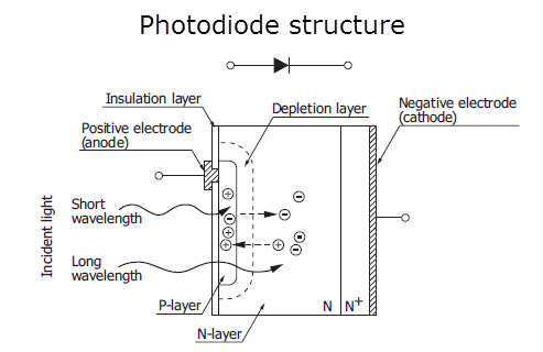
Figure 3. Structure of a photodiode.
An electrical equivalent circuit of a PD consists of a parallel combination of a current source (producing photocurrent that is linearly proportional to the power of the incident light), ideal diode (described by the Shockley equation), resistor (representing the resistance of the depletion region, also known as shunt resistance or junction resistance), and a capacitor (representing the capacitance of the depletion region, also known as junction capacitance). This parallel combination is in series with a resistor (representing the combined resistance of the undepleted regions of the PD, also known as series resistance).
A PD can be operated in three distinct modes. In the first, known as open circuit operation, an unbiased PD produces a voltage across its terminals. This open-circuit voltage is logarithmically proportional to the photocurrent. In the second mode, known as short circuit operation, the anode and cathode of a PD are connected together either with an electrical short (no bias) or with a voltage source that applies a reverse bias. In both cases, there is no load resistor to convert the output current to voltage. In this mode, the current in the electrical short is approximately equal to the photocurrent. In the third mode of operation, a PD is in series with a load resistor and voltage source. In the majority of cases, the voltage source reverse-biases the PD and the resistor converts a current signal to a voltage signal.
Avalanche photodiodes (APD)
An APD, portrayed in Figure 4, is a type of a PD that has an internal gain due to impact ionization of lattice atoms by charge carriers in the high-field section of the depletion region. A photo-generated charge carrier diffuses into the high-field region (or avalanche region) where it gains enough energy from the applied electric field to impact-ionize a lattice atom, creating additional charge carriers. The resulting charge carriers, while drifting through the avalanche region, can ionize more atoms, leading to the generation of even more charge carriers. In a typical operation, an APD is reverse-biased so that the operating point is in the breakdown region of its I-V characteristic. A gain up to about 100 is possible. If the reverse voltage is less than the breakdown voltage, an avalanche triggered by a single charge carrier ends by itself; otherwise, the avalanche must be externally ended or quenched. The latter mode of operation is known as Geiger mode.
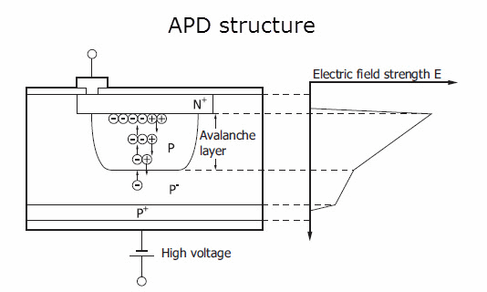
Figure 4. Structure of an avalanche photodiode (APD).
The gain of an APD is sensitive to fluctuations in biasing voltage and temperature. A user needs to stabilize both influences in an experimental setup where gain stability is vital. A possible approach is using an APD module, which contains, among others, circuitry for stabilizing temperature and voltage.
In a photon counting setup, an APD operates in Geiger mode — the reverse bias is greater than its breakdown voltage. In this application, an avalanche in an APD must be quenched by either a resistor connected in series with the APD (this is passive quenching) or by a more complex circuitry (this is active quenching).
Silicon photomultipliers (SiPM)
A SiPM is a rectangular array of square cells (pixels) where each cell is a series combination of an APD and a quenching resistor (see Figure 5). All of the cells are in a parallel combination. In a typical operation, a SiPM is reverse-biased so that the APDs operate in Geiger mode, giving the device a gain that is comparable to that of a PMT. One may think of a SiPM as a solid-state analog of a PMT, albeit with higher internal noise.
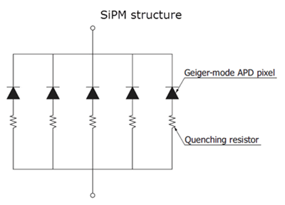
Figure 5. Structure of a silicon photomultiplier (SiPM).
A SiPM can be operated in both analog and digital modes, though the latter is more common. As a photon counter, a SiPM competes with a PMT. Its immunity to magnetic fields, lower operating voltage, ruggedness, and lower price are some of the advantages over a PMT; smaller active area, higher noise, and temperature sensitivity are some of the disadvantages.
Selecting a photodetector using the WITS$ approach
In the majority of cases, four traits of the light to be detected constrain the selection of an appropriate photodetector. They are spectral composition (what wavelengths of light are present?), intensity (how much light is there?), temporal behavior (is it a DC, AC, or pulsed light?), and spatial distribution (is the light collimated or diffuse?). The signal-to-noise ratio (S/N) at the output of a photodetector is a figure of merit that determines which photodetector performs best for the given input light. If the selection process yields more than one outstanding performer, the cost can be the additional selection criterion.
Selection based on wavelength
Key points
- Matching the spectrum of the observed light with the spectral responsivity of a photodetector is the first step in the selection process.
- Spectral responsivity σ(λ) expresses the efficacy with which a PMT, PD, or APD converts the incident radiant power to photocurrent.
- Quantum efficiency η(λ) and spectral responsivity are related to each other.
- Photon detection efficiency of a SiPM expresses the detected fraction of the incident photons. It is a function of wavelength and overvoltage.
The first step in the selection process is matching the spectrum of the observed light with the spectral sensitivity of a potential photodetector. The pertinent characteristic to be inspected is the detector's quantum efficiency as a function of wavelength η(λ) or, alternatively, responsivity σ(λ). The latter is also known as spectral sensitivity or, simply, photosensitivity. Quantum efficiency is a ratio of the number of photo-generated charge carriers per unit time contributing to the output signal to the number of incident photons on the light-sensitive section of the photodetector per unit time. Responsivity is a quotient of the electric current I (photocurrent, in Amperes) resulting from the photo-conversion and the incident optical power (in Watts). For a given wavelength, the two quantities are related by:
Equation 1
Hamamatsu provides at least one of these two quantities in the form of a plot as a function of wavelength (see Figure 6). Based on the "W" criterion only, the responsivity of the optimal photodetector would be higher than that of a competing photodetector at the wavelength of observed light. Ideally, this responsivity would also be close to or equal to the peak responsivity of the optimal detector. If a photodetector has zero responsivity at the wavelength of interest, the detector must not be selected no matter what its other characteristics are.
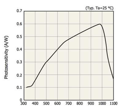
Figure 6. Example plot of spectral sensitivity as a function of wavelength provided by Hamamatsu for S1223 PIN PD. Note the maximum photosensitivity for λ ≈ 975 nm.
Photon detection efficiency (PDE) is an attribute of a SiPM that expresses the fraction of the incoming photons contributing to the output signal. It is a product of η(λ), fill factor (ratio of the light‐sensitive area to the total area), and the probability of avalanche. Hamamatsu provides plots of PDE as a function of wavelength and overvoltage (bias voltage minus breakdown voltage). If the PDE were zero at the wavelength of interest, a SiPM would not be an appropriate selection.
The first row in Table 1 gives the spectral coverage for the four families of photodetectors. None has photosensitivity for λ < 115 nm, but using scintillation techniques could make the detection of such radiation possible. PDs have the widest spectral coverage: their photosensitivity extends into far infrared; operating in this spectral region almost always requires cooling, in some cases, to a temperature of liquid nitrogen or lower.
The second row in Table 1 lists the peak quantum efficiency. The physical structure of the device and the type of light-sensitive material used in making the device control the wavelength of maximum quantum efficiency. The values show that solid-state devices have higher peak quantum efficiency when compared to PMTs.
Example
The typical cathode photosensitivity of Hamamatsu R374 PMT is σ = 64 mA/W at λ= 420 nm. What is the corresponding quantum efficiency at this wavelength?
Using Equation 1, one gets:
Quantum efficiency is 19% at λ = 420 nm.
Example
An experimenter needs to detect monochromatic radiation with λ = 2,000 nm = 2 μm. What photodetectors may be considered for this detection?
Table 1 implies that only PDs have photosensitivity at the observed wavelength. After inspecting a Hamamatsu catalog, an InGaAs PD G12183 is a possible choice (σ = 1.24 A/W, η = 77%) based on wavelength alone. Several other PDs similar to G12183 are also feasible.
Selection based on intensity
Key points
- Estimate the S/N at the photodetector's output for the given input light intensity, and determine which photodetector gives the highest S/N possible.
- The incident light power must be greater than the minimum detectable power for the detector to be a viable selection.
The second step in the selection process is estimating the S/N at the output of the photodetector for the given intensity of incident light, which the potential user needs to know, at least approximately. The desired outcome is the highest possible S/N.
There are two definitions of radiant intensity used in literature, which are not equivalent. In the first definition, it is the radiant power per unit solid angle, and, in the second, it is the radiant power passing a unit area. The latter is more appropriately known as irradiance I (in W⋅m-2). Suppose that a monochromatic light with constant irradiance illuminates a photodetector with active area A. The rate nγ with which the photons arrive at the surface is:
Equation 2
where Eγ = hc/λ is the energy of a single photon, P = IA is power of the incident light, h is Planck's constant, and c is the speed of light. The resulting rate of charge carrier photogeneration in the detector is given by:
Equation 3
The output signal from a photodetector can be viewed as a chronological sequence of current pulses, each originating from a single photo-generated charge carrier. Equations 2 and 3 imply that ne depends linearly on the product of I and A, thus, P. Maximizing S/N may comprise of maximizing the signal S and/or of minimizing the noise N. For a given I, increasing S may be possible by increasing P with light-collection optics or by selecting a photodetector with a larger active area. Decreasing N may be possible by selecting a detector with lower inherent noise and/or by limiting the detection bandwidth. Hamamatsu provides written guides and personal assistance on how to estimate the minimum detectable power — an input optical power yielding S/N = 1 at the output of the detector. A datasheet for a photodetector is likely to list noise equivalent power (NEP, in units of W/√Hz), which is the incident optical power that generates a photocurrent equal to the rms noise current for 1 Hz bandwidth. NEP is a function of wavelength and is given by:
Equation 4
A datasheet gives NEP for the peak wavelength; however, knowing σ(λ), NEP for other wavelengths can be calculated. NEP is useful for comparing photodetectors: all else being equal, a photodetector with a lower NEP yields a higher output S/N for the given power of the incident light.
Example
The datasheet for Hamamatsu S1223 PD states that NEP = 9.4 x 10⁻¹⁵ W/Hz1/2 for the peak wavelength λp = 960 nm.
a. What is the value of NEP for λ = 600 nm?
From the datasheet, σ(λ = 600 nm) = 0.4 A/W, thus:
b. If the detection bandwidth B = 100 kHz, what is the minimum detectable power (ignoring photon shot noise) for λ = 600 nm?
c. What irradiance does the answer to the above question imply?
From the datasheet, the active area A = 2.4 x 2.8 mm2. Thus, the implied irradiance is:
NEP is proportional to the square root of both electrical bandwidth and the photodetector area. A figure of merit known as specific detectivity D*, defined as
Equation 5
factors out these dependencies, making D* very useful in comparing photoresponse of detectors in the same family. It is commonly given in the form of a plot as a function of wavelength (see Figure 7) for IR photodetectors.
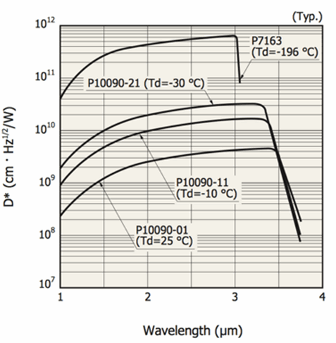
Figure 7. Specific detectivity as a function of wavelength for InAs photovoltaic IR detectors.
Example
Figure 7 shows D*(λ) for, among others, P7163 InAs PD. The figure is from the datasheet for this detector.
What is the minimum detectable power (ignoring photon shot noise) at λ = 2,000 nm = 2 μm for B = 1 Hz? What would it be for B = 1 kHz? Assume that the detector is cooled to -196°C.
From Figure 7, D* = 4.5 x 1011 cm⋅Hz1/2/W at 2 μm. From the datasheet, the diameter of the active area is 1 mm, which implies an area of 7.9 x 10⁻³ cm2. Using Equation 5, NEP is
The value of Pmin increases as √B; thus for 1 kHz bandwidth, Pmin ≈ 6 pW.
Example
Suppose that the incident power (monochromatic light, λ = 2 μm) on P7163 is 70 pW. What is the resulting S/N for 1 kHz detection bandwidth? Assume that the detector is cooled to ‐196°C.
From the datasheet, D* = 6 x 1011 cm⋅Hz1/2/W and σ = 1.3 A/W at peak wavelength (λp = 3 μm). D* = 4.5 x 1011 cm⋅Hz1/2/W for λ = 2 μm. Thus, σ at λ = 2 μm is given by
One can show that for a PD, S/N can be given by the following relationship
Equation 6
and after substituting the relevant quantities, Equation 6 yields
The signal is detectable.
Figure 8 depicts the suitability of selecting a photodetector depending on the input light level. The scaling for the top axis corresponds to the photon irradiance [number of photons ⋅ mm-2 ⋅ s-1]. The axis below gives the corresponding irradiance (in W ⋅ mm-2) assuming monochromatic light with λ = 550 nm. The bottom axis gives a distance R (in m) from a 1 W point source producing the above irradiances. Suppose that each photodetector has an active area equal to or larger than 1 mm2 and that it is spot illuminated with an effective beam size of 1 mm2. In this case, the rate of the photon arrival nγ is equal to 1 mm2 times the photon irradiance. If nγ is less than about 108 s-1, the current pulses are distinguishable in time and detecting them individually is known as photon counting. The horizontal red line in the figure depicts this regime. A blue arrow indicates the range of irradiances that a given photodetector can detect.
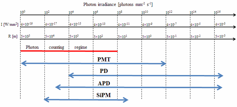
Figure 8. Photodetector sensitivity to light levels.
A PMT is the best choice — perhaps the only choice — for situations where the incident light level is extremely low. As the light level increases, a SiPM, an APD, and finally, a PD become viable choices. Where the detectors overlap, other characteristics of light and the detector should be considered in making the selection. For high light levels, a PD and an APD are the possible choices; however, in a vast number of cases, a PD will be the better choice when ease of use and device cost are taken into consideration.
Example
A collimated beam of monochromatic light (λ = 450 nm) has an irradiance I = 1 pW/m2.
a. Which photodetector will produce a larger photocurrent: a PMT with a circular photocathode with 15‐mm diameter and quantum efficiency ηPMT = 18%, or a 10 x 10 mm2 PD with quantum efficiency η = 60%? Assume that the incident beam is wider than the area of either photodetector.
Combining Equations 2 and 3, the ratio of the rate at which photoelectrons are produced in a PMT to the rate at which charge carriers are produced in a PD is
The rate of charge generation in a PD is larger than that in a PMT, and the result is independent of the irradiance.
b. How many photons per second strike each photodetector?
Using Equation 2, nPMTγ = 1.1 x 10³ photons/s and nPDγ = 0.6 x 10³ photons/s. This is a photon counting regime.
c. Which of the two detectors would be a better choice?
The PMT. Despite the smaller photocurrent, the lower internal noise of the PMT makes it a better choice.
Before moving on to the next selection criterion, it is important to note several points.
- A complete estimate of S/N should include contribution to noise from the detection circuit (e.g., a resistor or transimpedance amplifier). This contribution becomes less significant for a photodetector with internal gain, and this fact alone is the reason for a gain in a photodetector.
- The minimum detectable power is a function of detection bandwidth. Higher bandwidth increases noise and, therefore, increases the minimum detectable power. Alternatively, higher bandwidth lowers S/N for a given power of input light.
- Large bandwidth is desirable if high fidelity is required: the output electrical signal accurately reproduces the input light signal.
- The minimum detectable power for a given bandwidth is always larger than NEP for the same bandwidth because NEP does not include signal photon shot noise.
- Terminal capacitance of the photodetector affects the detection bandwidth: the higher the capacitance, the smaller the bandwidth.
- For the solid-state photodetectors (but not for PMTs), a larger active area causes a larger terminal capacitance, which decreases the detection bandwidth. Consequently, there is a tradeoff between sensitivity and bandwidth, or sensitivity and signal fidelity.
Selection based on temporal characteristic of incident light
Key points
- DC input light has a constant intensity. The intensity of an AC input light varies with time. A pulsed input light arrives as discrete packets of photons.
- For AC and pulsed light, the capacitance of a photodetector affects the rise time, time jitter, and detection bandwidth.
- Dynamic range and linearity should also be taken into account in pulsed and AC light.
The intensity of the incident light can be a function of time. It is a DC light if the intensity is constant, AC light if the intensity varies with time, and pulsed light if it arrives as discrete packets of photons. A DC light poses no additional restrictions on the photodetector but the other two do. For AC and pulsed light, capacitances — junction, parasitic, or terminal — matter: their values affect the output signal rise time, time jitter, and detection bandwidth. Table 1 lists these parameters: the rise time and bandwidth are for a 50 Ω resistive load (current-to-voltage conversion), whereas time jitter is for a single-photon illumination. Increasing the load resistance increases the output voltage but reduces the bandwidth. Because the quantity of noise in the output increases with bandwidth, a well-designed system has just enough bandwidth for the purpose of the observation.
A detector's rise time tr and its bandwidth B are related by a well-known approximate equation
Equation 7
where B is in GHz and tr is in ns. The rise time of a photodetector is measured using monochromatic δ‐like illumination. The measured value of tr depends on the operating conditions of a detector. In the case of a PMT, tr decreases with increasing bias voltage, and in the case of PD, APD, and SiPM, it decreases as the reverse voltage increases. Detection electronics (a load resistor, transimpedance amplifier, or charge amplifier) also affect tr and, thus B. For the simplest case of a load resistor RL, B ∝ (RLCt)-1, where Ct is terminal capacitance. The higher the values of RL and Ct, the smaller the bandwidth.
Dynamic range and a related concept, linearity, of a photodetector should also be examined in pulsed and AC detection. Is there enough dynamic range to detect the full variation of the incident intensity? Are the input and output signals linearly related — if not, what is the deviation and is it acceptable? Several factors can influence the dynamic range of a photodetector. A few among them are an intrinsic noise floor, biasing level, output load, and, in the case of a SiPM, number of cells. Hamamatsu provides information on dynamic range and linearity most commonly in the form of graphs, for example, linearity versus the power of incident light or linearity versus the load resistance.
Example
An experimenter narrowed a choice of detectors to two Hamamatsu photodetectors for high-frequency detection: R9880U-20 PMT and S3399 PD. The experimental conditions are monochromatic light (λ = 800 nm), sinusoidally modulated (frequency of modulation ƒm = 50 MHz), and adjustable maximum and minimum irradiance to meet detectability and linearity constraints of a detector. A 50 Ω load resistor will be used to perform current-to-voltage conversion at the output. Which detector should the experimenter select?
Since the irradiance of the input light can be adjusted to satisfy linearity and detectability requirements of a detector, the higher quantum efficiency of S3399 is not an advantage nor is the larger photosensitive area of R9880U‐20. The crucial comparison is the bandwidth. At the recommended biasing, tr = 0.57 ns for the PMT, implying B = 610 MHz. While reverse-biased to 10 V, B = 100 MHz for the PD. In both cases, the values of B are for a 50 Ω termination. The PD, which is easier to operate and less expensive than the PMT, has enough bandwidth for the required detection and would be an appropriate selection.
Example
Suppose that the incident light from the previous example is now modulated with a square wave having 50% duty cycle and a modulation frequency ƒm = 50 MHz. It is important in the experimental setup that the output has the highest possible signal fidelity. Which of the two photodetectors is a better choice in this case?
The Fourier representation of the 50 MHz square wave contains odd-integer harmonic frequencies (in addition to the fundamental frequency of 50 MHz): 150 MHz, 250 MHz, 350 MHz, etc. Given that the output signal fidelity is the primary requirement, the PMT is a better choice because of its larger bandwidth.
Selection based on spatial characteristic of incident light
If the level of incoming light is low but the light is nearly collimated, employing focusing optics can increase the incident light power on the detector, and, thus, improve the S/N. If, however, the incoming light is diffuse, focusing optics will not increase the incident power (diffuse light cannot be focused); the only other option is to use a detector with a larger active area. The tradeoff is a higher dark current in the photodetector, which increases noise and, therefore, NEP. As discussed above, in the case of a PD, APD, and SiPM (but not PMT), a larger active area reduces the detection bandwidth due to a larger junction capacitance.
Selection based on price
Key points
- Price may be the tiebreaker if the selection based on wavelength, light intensity, time characteristics, and spatial characteristics did not point to only one detector.
- Typical costs of stand-alone detectors: PD < APD < SiPM < PMT.
If the selection process based on WITS did not yet produce a unique and outstanding choice (unlikely but possible), the price may be able to break the tie. The prices can vary greatly among the different models of a photodetector in a given family; however, when the typical representatives of the families are compared, the highest to lowest prices are for a PMT, SiPM, APD, and PD. This is a price for a stand-alone photodetector. If the potential user needs to design the detection setup from the ground up, the cost of auxiliary equipment such as power supplies, amplifiers, etc. should also be considered. All of the detectors described in this article are also offered as part of a module. Together with the photodetector, a module may or may not contain, for example, a power supply, amplifier, temperature and/or voltage control system, or an A-to-D converter.
Although in most cases the selection process would end here, there are applications and situations where additional criteria need to be considered. Examples are ruggedness, immunity to an external magnetic field, ease of use, physical size, and ease of customization. If the device may be customized, how much does it cost? How long is the lead time?
The selection process can be taxing, confusing, and potentially costly. Establishing a partnership with the device manufacturer can make the process much quicker and results in the optimal selection.
Products referenced in this article
Notes
- An abridged version of this article was published in the July 2015 issue of Industrial Photonics.
- Confirmation
-
It looks like you're in the . If this is not your location, please select the correct region or country below.
You're headed to Hamamatsu Photonics website for US (English). If you want to view an other country's site, the optimized information will be provided by selecting options below.
In order to use this website comfortably, we use cookies. For cookie details please see our cookie policy.
- Cookie Policy
-
This website or its third-party tools use cookies, which are necessary to its functioning and required to achieve the purposes illustrated in this cookie policy. By closing the cookie warning banner, scrolling the page, clicking a link or continuing to browse otherwise, you agree to the use of cookies.
Hamamatsu uses cookies in order to enhance your experience on our website and ensure that our website functions.
You can visit this page at any time to learn more about cookies, get the most up to date information on how we use cookies and manage your cookie settings. We will not use cookies for any purpose other than the ones stated, but please note that we reserve the right to update our cookies.
1. What are cookies?
For modern websites to work according to visitor’s expectations, they need to collect certain basic information about visitors. To do this, a site will create small text files which are placed on visitor’s devices (computer or mobile) - these files are known as cookies when you access a website. Cookies are used in order to make websites function and work efficiently. Cookies are uniquely assigned to each visitor and can only be read by a web server in the domain that issued the cookie to the visitor. Cookies cannot be used to run programs or deliver viruses to a visitor’s device.
Cookies do various jobs which make the visitor’s experience of the internet much smoother and more interactive. For instance, cookies are used to remember the visitor’s preferences on sites they visit often, to remember language preference and to help navigate between pages more efficiently. Much, though not all, of the data collected is anonymous, though some of it is designed to detect browsing patterns and approximate geographical location to improve the visitor experience.
Certain type of cookies may require the data subject’s consent before storing them on the computer.
2. What are the different types of cookies?
This website uses two types of cookies:
- First party cookies. For our website, the first party cookies are controlled and maintained by Hamamatsu. No other parties have access to these cookies.
- Third party cookies. These cookies are implemented by organizations outside Hamamatsu. We do not have access to the data in these cookies, but we use these cookies to improve the overall website experience.
3. How do we use cookies?
This website uses cookies for following purposes:
- Certain cookies are necessary for our website to function. These are strictly necessary cookies and are required to enable website access, support navigation or provide relevant content. These cookies direct you to the correct region or country, and support security and ecommerce. Strictly necessary cookies also enforce your privacy preferences. Without these strictly necessary cookies, much of our website will not function.
- Analytics cookies are used to track website usage. This data enables us to improve our website usability, performance and website administration. In our analytics cookies, we do not store any personal identifying information.
- Functionality cookies. These are used to recognize you when you return to our website. This enables us to personalize our content for you, greet you by name and remember your preferences (for example, your choice of language or region).
- These cookies record your visit to our website, the pages you have visited and the links you have followed. We will use this information to make our website and the advertising displayed on it more relevant to your interests. We may also share this information with third parties for this purpose.
Cookies help us help you. Through the use of cookies, we learn what is important to our visitors and we develop and enhance website content and functionality to support your experience. Much of our website can be accessed if cookies are disabled, however certain website functions may not work. And, we believe your current and future visits will be enhanced if cookies are enabled.
4. Which cookies do we use?
There are two ways to manage cookie preferences.
- You can set your cookie preferences on your device or in your browser.
- You can set your cookie preferences at the website level.
If you don’t want to receive cookies, you can modify your browser so that it notifies you when cookies are sent to it or you can refuse cookies altogether. You can also delete cookies that have already been set.
If you wish to restrict or block web browser cookies which are set on your device then you can do this through your browser settings; the Help function within your browser should tell you how. Alternatively, you may wish to visit www.aboutcookies.org, which contains comprehensive information on how to do this on a wide variety of desktop browsers.
5. What are Internet tags and how do we use them with cookies?
Occasionally, we may use internet tags (also known as action tags, single-pixel GIFs, clear GIFs, invisible GIFs and 1-by-1 GIFs) at this site and may deploy these tags/cookies through a third-party advertising partner or a web analytical service partner which may be located and store the respective information (including your IP-address) in a foreign country. These tags/cookies are placed on both online advertisements that bring users to this site and on different pages of this site. We use this technology to measure the visitors' responses to our sites and the effectiveness of our advertising campaigns (including how many times a page is opened and which information is consulted) as well as to evaluate your use of this website. The third-party partner or the web analytical service partner may be able to collect data about visitors to our and other sites because of these internet tags/cookies, may compose reports regarding the website’s activity for us and may provide further services which are related to the use of the website and the internet. They may provide such information to other parties if there is a legal requirement that they do so, or if they hire the other parties to process information on their behalf.
If you would like more information about web tags and cookies associated with on-line advertising or to opt-out of third-party collection of this information, please visit the Network Advertising Initiative website http://www.networkadvertising.org.
6. Analytics and Advertisement Cookies
We use third-party cookies (such as Google Analytics) to track visitors on our website, to get reports about how visitors use the website and to inform, optimize and serve ads based on someone's past visits to our website.
You may opt-out of Google Analytics cookies by the websites provided by Google:
https://tools.google.com/dlpage/gaoptout?hl=en
As provided in this Privacy Policy (Article 5), you can learn more about opt-out cookies by the website provided by Network Advertising Initiative:
http://www.networkadvertising.org
We inform you that in such case you will not be able to wholly use all functions of our website.
Close