Application notes

Technical notes
Ask an engineer


Publications
United States (EN)
Select your region or country.
ORCA®-Quest Questions & Answers
What makes the ORCA-Quest camera unique?
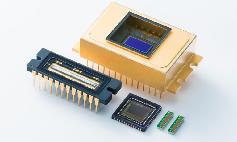
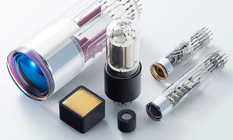
The ORCA-Quest quantitative CMOS (qCMOSⓇ) camera with photon number resolving functionality is the leap in scientific camera evolution that transforms imaging into imagining (Fig. 1). With ultra-quiet, highly refined electronics, this camera is more than an image capture device; it is a precision instrument that unlocks the ability to investigate new photonic questions because it offers the quality and quantitative performance to detect meaningful data previously lost in the noise. The ORCA-Quest is the world's first camera to incorporate the qCMOS image sensor and to be able to resolve the number of photoelectrons. It features extremely low noise, high quantum efficiency, large area, and high-speed readout.
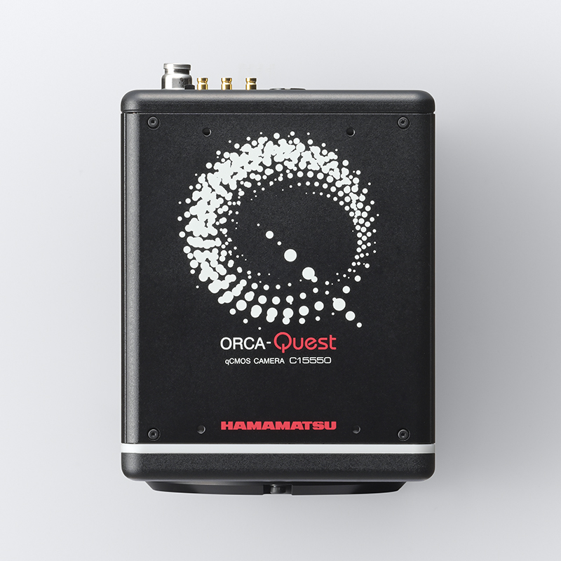
Figure 1. ORCA-Quest quantitative CMOS (qCMOS) camera
What is photon number resolving?
First, let’s be clear: as with any digital imaging device, what is being detected and measured are photoelectrons. Resolving individual photo(electro)ns has primarily been the domain of point detectors such as photomultiplier tubes (PMTs) and avalanche photodiodes (APDs). Photon counting is a measurement technique that relies on the properties of these detectors to indicate whether a photon (or two) has been detected with some level of certainty. But they cannot “count” photons much beyond the threshold of a binary yes or no. In Photon Number Resolving Mode, the ORCA-Quest quantitative CMOS (qCMOS) camera outputs actual counts of photoelectrons per pixel up to a max of 200 photoelectrons (Fig. 2). Single-photon sensitivity in a camera is not achieved through a single specification. To count these photoelectrons, the camera noise must be sufficiently smaller than the amount of photoelectron signal. Conventional sCMOS cameras achieve a small readout noise, but still larger than the photoelectron signal, making it difficult to count photoelectrons.
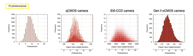
Figure 2. Comparison of photon number resolving capability
What is camera noise?
Simplistically, read noise is pixel variation in the conversion of a charge to a digital signal. Each pixel’s photoelectron charge must be detected, converted to voltage, amplified, and digitized. Each of these steps has error associated with it. Read noise is specified as electrons rms to capture in one number the most meaningful spec. But in a camera with 9.4 megapixels, the pixel-to-pixel variation in read noise across the sensor and/or in a single pixel over time can impact image quality and data analysis.
The ORCA-Quest quantitative CMOS (qCMOS) camera pushes that boundary even further and, as can be seen in Fig. 3, has a very narrow read noise distribution, minimizing the salt and pepper visual effect of noisy pixels that can also wreak havoc on computational techniques such as precision localization super-resolution. To detect weak light with a high signal-to-noise ratio, every aspect of the ORCA-Quest, from its sensor structure to its electronics, has been optimally designed. Not only the camera development but also the custom sensor development has been done with the latest qCMOS technology, resulting in extremely low noise performance of 0.27 electrons rms.
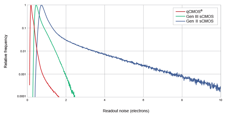
Figure 3. Readout noise comparison
How does back-thinning work?
A traditional, front-illuminated digital camera is constructed in a fashion similar to the human eye, with a lens at the front and photodetectors at the back. This traditional orientation of the sensor places the active area of the digital camera image sensor on its front surface. The matrix and its wiring reflect a portion of the input photons, and the active area can only receive part of the incoming photons. The reflection reduces the signal that is available to be captured. A back-illuminated sensor contains the same elements, but arranges the wiring behind the active area by flipping the silicon wafer during manufacturing, then thinning its reverse side so that light can hit the active area without passing through the wiring layer. This change can improve the chance of an input photon being captured from about 60% to over 90%.
Back-thinning CCDs for enhanced quantum efficiency (QE) has been done for decades, and EM-CCDs are an example of back-thinned technology becoming commonplace. There are two tradeoffs around back-thinning that are often underestimated: etaloning and impaired resolution as measured by the modulation transfer function (MTF). As with any transformative new product, clever new features take the headlines. But often it is the minimization of age-old nagging issues that frees up the technology for greatness.
What is etaloning?
Etaloning is a phenomenon that occurs when the incident light interferes with the reflected light from the back surface of the silicon and causes varying sensitivity. This is dependent on both the spatial and the spectral. In the case of an EM-CCD camera, it appears as a fringe pattern even with uniform monochrome light input, mostly in the IR. The quantitative CMOS (qCMOS) camera shows minimal etaloning compared to EM-CCD cameras (Fig. 4).
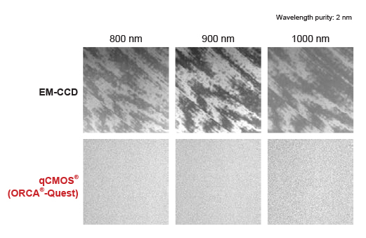
Figure 4. Etaloning comparison
What is MTF?
The modulation transfer function (MTF) is a way to characterize resolution and performance. The MTF indicates how much of the object's contrast is captured in the image as a function of spatial frequency. Resolution is typically considered as the overall number of pixels and pixel size, but pixel structure can also play a role in functional resolution. Every pixel is expected to collect light only from an optically specified area. But if the incoming photons from that area create charge in an adjacent pixel, then there is crosstalk among the pixels and deterioration of resolution. By creating a deep trench isolation structure in the pixel design of the ORCA-Quest quantitative CMOS camera, crosstalk is minimized. This improvement is measured by calculating how many patterned lines of contrasting light and dark can be resolved in a given area. Compared to back-illuminated sCMOS and EM-CCD cameras, the ORCA-Quest shows noticeable improvement in MTF that will produce greater sharpness in images at all magnifications (Fig. 5).
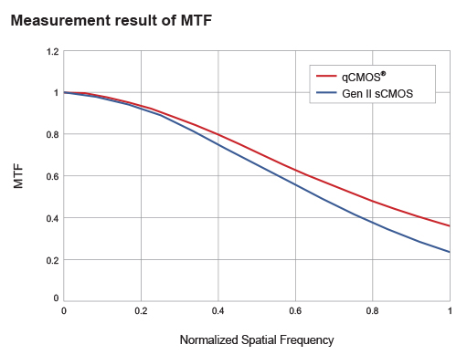
Figure 5. MTF (modulation transfer function) comparison
If you have a technical question you’d like to see answered on this page, email us.
Meet the engineer

Brad Coyle has been working in imaging for over 15 years. He joined Hamamatsu 6 years ago and is currently an OEM Camera Product Manager. His expertise includes camera and sensor technologies, and advanced imaging applications. In his spare time, he enjoys playing soccer, cooking, and hiking with his family.
- Confirmation
-
It looks like you're in the . If this is not your location, please select the correct region or country below.
You're headed to Hamamatsu Photonics website for US (English). If you want to view an other country's site, the optimized information will be provided by selecting options below.
In order to use this website comfortably, we use cookies. For cookie details please see our cookie policy.
- Cookie Policy
-
This website or its third-party tools use cookies, which are necessary to its functioning and required to achieve the purposes illustrated in this cookie policy. By closing the cookie warning banner, scrolling the page, clicking a link or continuing to browse otherwise, you agree to the use of cookies.
Hamamatsu uses cookies in order to enhance your experience on our website and ensure that our website functions.
You can visit this page at any time to learn more about cookies, get the most up to date information on how we use cookies and manage your cookie settings. We will not use cookies for any purpose other than the ones stated, but please note that we reserve the right to update our cookies.
1. What are cookies?
For modern websites to work according to visitor’s expectations, they need to collect certain basic information about visitors. To do this, a site will create small text files which are placed on visitor’s devices (computer or mobile) - these files are known as cookies when you access a website. Cookies are used in order to make websites function and work efficiently. Cookies are uniquely assigned to each visitor and can only be read by a web server in the domain that issued the cookie to the visitor. Cookies cannot be used to run programs or deliver viruses to a visitor’s device.
Cookies do various jobs which make the visitor’s experience of the internet much smoother and more interactive. For instance, cookies are used to remember the visitor’s preferences on sites they visit often, to remember language preference and to help navigate between pages more efficiently. Much, though not all, of the data collected is anonymous, though some of it is designed to detect browsing patterns and approximate geographical location to improve the visitor experience.
Certain type of cookies may require the data subject’s consent before storing them on the computer.
2. What are the different types of cookies?
This website uses two types of cookies:
- First party cookies. For our website, the first party cookies are controlled and maintained by Hamamatsu. No other parties have access to these cookies.
- Third party cookies. These cookies are implemented by organizations outside Hamamatsu. We do not have access to the data in these cookies, but we use these cookies to improve the overall website experience.
3. How do we use cookies?
This website uses cookies for following purposes:
- Certain cookies are necessary for our website to function. These are strictly necessary cookies and are required to enable website access, support navigation or provide relevant content. These cookies direct you to the correct region or country, and support security and ecommerce. Strictly necessary cookies also enforce your privacy preferences. Without these strictly necessary cookies, much of our website will not function.
- Analytics cookies are used to track website usage. This data enables us to improve our website usability, performance and website administration. In our analytics cookies, we do not store any personal identifying information.
- Functionality cookies. These are used to recognize you when you return to our website. This enables us to personalize our content for you, greet you by name and remember your preferences (for example, your choice of language or region).
- These cookies record your visit to our website, the pages you have visited and the links you have followed. We will use this information to make our website and the advertising displayed on it more relevant to your interests. We may also share this information with third parties for this purpose.
Cookies help us help you. Through the use of cookies, we learn what is important to our visitors and we develop and enhance website content and functionality to support your experience. Much of our website can be accessed if cookies are disabled, however certain website functions may not work. And, we believe your current and future visits will be enhanced if cookies are enabled.
4. Which cookies do we use?
There are two ways to manage cookie preferences.
- You can set your cookie preferences on your device or in your browser.
- You can set your cookie preferences at the website level.
If you don’t want to receive cookies, you can modify your browser so that it notifies you when cookies are sent to it or you can refuse cookies altogether. You can also delete cookies that have already been set.
If you wish to restrict or block web browser cookies which are set on your device then you can do this through your browser settings; the Help function within your browser should tell you how. Alternatively, you may wish to visit www.aboutcookies.org, which contains comprehensive information on how to do this on a wide variety of desktop browsers.
5. What are Internet tags and how do we use them with cookies?
Occasionally, we may use internet tags (also known as action tags, single-pixel GIFs, clear GIFs, invisible GIFs and 1-by-1 GIFs) at this site and may deploy these tags/cookies through a third-party advertising partner or a web analytical service partner which may be located and store the respective information (including your IP-address) in a foreign country. These tags/cookies are placed on both online advertisements that bring users to this site and on different pages of this site. We use this technology to measure the visitors' responses to our sites and the effectiveness of our advertising campaigns (including how many times a page is opened and which information is consulted) as well as to evaluate your use of this website. The third-party partner or the web analytical service partner may be able to collect data about visitors to our and other sites because of these internet tags/cookies, may compose reports regarding the website’s activity for us and may provide further services which are related to the use of the website and the internet. They may provide such information to other parties if there is a legal requirement that they do so, or if they hire the other parties to process information on their behalf.
If you would like more information about web tags and cookies associated with on-line advertising or to opt-out of third-party collection of this information, please visit the Network Advertising Initiative website http://www.networkadvertising.org.
6. Analytics and Advertisement Cookies
We use third-party cookies (such as Google Analytics) to track visitors on our website, to get reports about how visitors use the website and to inform, optimize and serve ads based on someone's past visits to our website.
You may opt-out of Google Analytics cookies by the websites provided by Google:
https://tools.google.com/dlpage/gaoptout?hl=en
As provided in this Privacy Policy (Article 5), you can learn more about opt-out cookies by the website provided by Network Advertising Initiative:
http://www.networkadvertising.org
We inform you that in such case you will not be able to wholly use all functions of our website.
Close