Application notes

Technical notes
Ask an engineer


Publications
United States (EN)
Select your region or country.
Advances in CMOS image sensors open doors to many industrial, scientific, and commercial imaging applications
Yakov Bulayev, Hamamatsu Corporation
September 2, 2015
Introduction
Since the invention of charge-coupled devices (CCD) in the 1970s, these devices have dominated the area of scientific and industrial imaging applications. However, in the 1990s monolithic complementary metal-oxide semiconductor (CMOS) arrays emerged as a serious alternative to CCD image sensors. This was the result of significant improvements in silicon CMOS technology that have been technically and economically driven by digital microelectronics (microprocessors, memory devices, etc.) and applications [1].
Until recently, CCD image sensors were the sensors of choice for most industrial and scientific applications, while applications of CMOS image sensors were primarily confined to consumer photography. However, recent advances in CMOS sensor technology have rendered these devices an effective imaging solution for numerous industrial, scientific, and commercial applications.
There are multiple functional and performance differences between CCD and CMOS image sensors. Understanding the key differences between these two image sensor technologies will allow distinguishing advantages and limitations of each type of device and help in selecting the optimal device for a given application.
CCD image sensors
A CCD image sensor consists of an array of photosensitive charge-coupled elements (pixels). The output signal of the sensor is proportional to the electrical charge accumulated by each pixel in response to irradiation.
Charge transport in a CCD imager is controlled by multiphase – usually two to four – signals that induce potential wells under the electrodes and control the motion of electron packets residing in the potential wells. Charge transport includes transferring charge packets in the columnar direction, as well as clocking off the charge through the horizontal (readout) register to the charge-measurement circuit and output amplifier. This procedure causes charge packets to exit the array of pixels one row at a time.
Among known architectural configurations of CCD imagers, three of the most popular are referred to as full-frame, frame transfer, and interline. The full-frame architecture, which provides a 100% fill factor, is the most universal CCD architecture used for scientific and industrial applications.
Depending on the required spectral response, CCD sensors can be designed for front or back illumination. In front-illuminated CCDs, light must pass through the polysilicon gate structure located above the photosensitive silicon layer called the “depletion layer.” However, variations in the refraction indices between the polysilicon and silicon structures cause shorter wavelength light to reflect off the CCD surface. This effect, combined with intense ultraviolet (UV) light absorption in the polysilicon, leads to diminished quantum efficiency (QE) for those wavelengths in the front-illuminated detectors. To improve the overall QE and enable increased CCD sensitivity at UV wavelengths, back-thinned technology can be used [2]. In back-thinned devices, also known as back-illuminated CCDs, the incident photon flux does not have to penetrate the polysilicon gates and is absorbed directly into the silicon pixels.
Concepts of CMOS image sensors
In CMOS arrays, photon-to-voltage conversion occurs inside each pixel. In general, a CMOS sensor consists of an array of identical pixels. Each pixel includes a photodiode and at least one transistor acting as a switch [3].
Originally CMOS sensors used the so-called passive pixel structure (Fig. 1a).
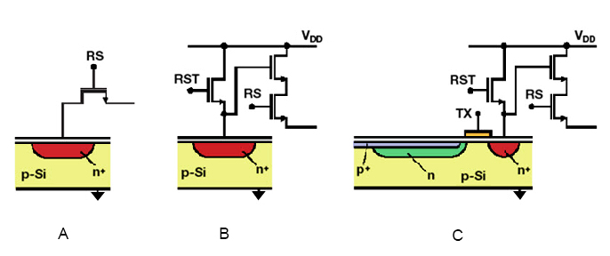
Figure 1. Structure of passive pixel (a), active pixel (b) and pinned photodiode pixel (c)
A passive pixel works as follows:
- At the beginning of an exposure, the photodiode is reverse-biased on reset.
- During the exposure time, impinging photons decrease the reverse voltage across the photodiode.
- At the end of exposure, the remaining voltage across the photodiode is measured; its drop from the original value is used as a measure of the amount of photons falling on the photodiode.
- The photodiode is reset to be prepared for the next exposure cycle.
The passive pixel sensor (PPS) is characterized by a large fill factor (the ratio of photodiode area to total pixel area), but it suffers from a high noise level. High noise is caused by the mismatch between the small capacitance of the pixel and the large capacitance of the signal bus.
A major improvement in the pixel noise performance was achieved by introducing the active pixel concept, which became very popular in the mid-1990s. In the active pixel sensor (APS), each pixel includes a photodiode, a reset transistor, an addressing transistor, and an amplifier, usually a source follower (Fig. 1b).
The principle of operation of the active pixel sensor is similar to that of the passive pixel sensor:
- The photodiode is reverse-biased on reset.
- Impinging photons decrease the reverse voltage across the photodiode.
- At the end of exposure, the pixel is addressed, and the source follower transmits the voltage across the diode outside the pixel.
- The photodiode is reset once again.
The active pixel structure solved a lot of noise issues. However, the kTC noise caused by resetting the photodiode persisted. To address this issue, further improvements to the pixel structure – such as adding a pinned photodiode and correlated double sampling (CDS) – were introduced.
The pinned photodiode (PPD) pixel shown in Fig. 1c was a logical improvement to the traditional APS. A pinned photodiode added to the pixel was separated from the readout node by means of a transfer gate TX. The PPD pixel has the following advantages in comparison with the traditional APS:
- Low noise performance achieved through correlated double sampling
- High sensitivity and low dark current of a photodiode
In a PPD pixel, conversion of the incoming photons is performed in the pinned photodiode. A PPD pixel operates as follows.
- At the end of exposure, the readout node is reset by the reset transistor.
- The output voltage is measured.
- The photodiode is drained by activating TX, and the photodiode signal is transferred to the readout node.
- The output voltage is measured again after the signal has been transferred.
- CDS signal processing is performed: the second voltage measurement is subtracted from the first measurement.
Since the active components can be integrated into pixels, the pixels can become fully addressable, and on-chip image processing can be performed. To denote the number of transistors in a pixel, the pixels are referred to as 3T, 4T, 5T, etc. As the number of transistors increases, functionality and operating flexibility increase, too. When it comes to improved performance, pixels with four or more transistors offer significant noise reductions.
In general, two types of noise – temporal and spatial – should be taken into account when considering an image sensor based design.
One important component of temporal noise which should be considered is the photon shot noise. The source of this noise is statistical variation in the amount of photons absorbed by the sensor during exposure [3]. This stochastic process can be described by Poisson statistics. Let’s assume that during the exposure a pixel receives an average amount of photons equal to μph. This average value is characterized by a noise component σph, representing the photon shot noise. The relationship between the average value μph and its associated noise can be described as:
Equation 1
After the absorption of incoming photons by a pixel, the flux of µph photons results in μe electrons stored in this pixel. These electrons are characterized by a noise component σe, which also has a square root relationship with µe. Assuming that we are dealing with a hypothetical noise-free imager and noise-free electronics, the performance of the image sensor based system will be limited by photon shot noise. The maximum signal-to-noise ratio can be described as follows:
Equation 2
Since the maximum signal-to-noise ratio equals the square root of the signal value, the minimum pixel dimensions will be limited not by the CMOS technology but by the number of electrons that can be stored in the pixel [3].
As noted above, advances in CMOS image sensor technology make CMOS image sensors suitable for numerous scientific, industrial and commercial applications.
There are two types of CMOS image sensors currently available on the market: CMOS linear image sensors and CMOS area (2D) image sensors.
CMOS linear image sensors
The typical CMOS linear image sensor includes a shift register, a linear photodiode array, an amplifier array, a hold circuit, a timing generator, and a bias circuit.
Improved features and characteristics of CMOS linear image sensors make them suitable for various applications including spectroscopy, machine vision, and barcode scanning.
For example, manufacturers of spectroscopy instruments welcomed the Hamamatsu S11639 CMOS linear image sensor (Fig. 2) as an alternative to CCD sensors.
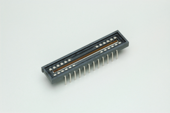
Figure 2. CMOS linear image sensor S11639
The pixel format of this active pixel sensor is optimized for spectroscopy applications. Also, most of its performance characteristics are comparable with those of the time-honored Sony ILX511 CCD sensor or exceed them [4]. This Hamamatsu sensor has a spectral response range from UV to NIR (Fig. 3) without the need for any additional coating and meets the requirements of spectroscopy systems for image sensors [5].
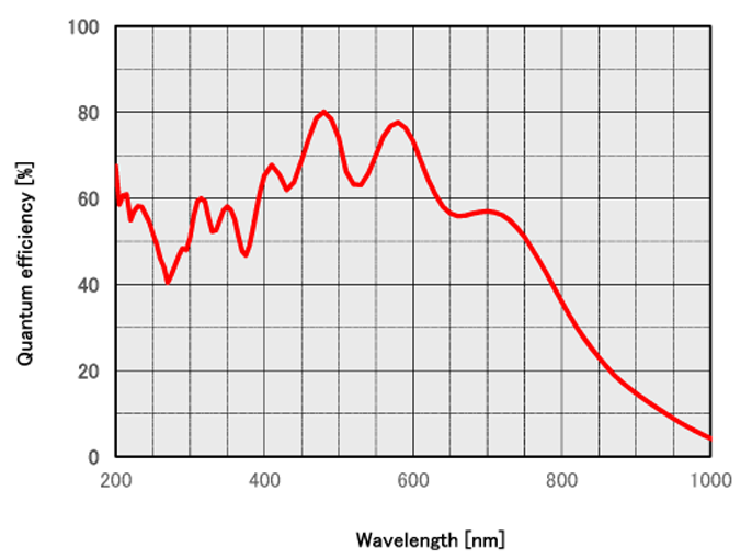
Figure 3. Spectral response of the S11639 sensor
In addition to spectroscopy applications, the S11639 sensor can also be used for position detection, image reading, encoding, and other machine vision applications.
One of the advantages of CMOS technology is that it allows integration into a CMOS sensor of different circuitries which perform signal processing, timing generation, analog-to-digital conversion, electronic shutter, variable integration time, interfacing, and other functions.
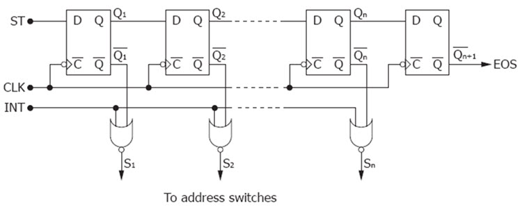
Figure 4. Shift register for readout control
For example, Hamamatsu offers a CMOS linear image sensor with a variable integration time function beneficial for some spectrophotometry instruments. This function is performed by means of an embedded shift register (Fig. 4) that allows resetting specific pixels during the readout cycle or letting the pixels absorb incoming photons without being reset until the next readout cycle. The ON or OFF condition of the address switches S1-Sn of each pixel is controlled by the INT signal that is synchronized with the clock signal (CLK).
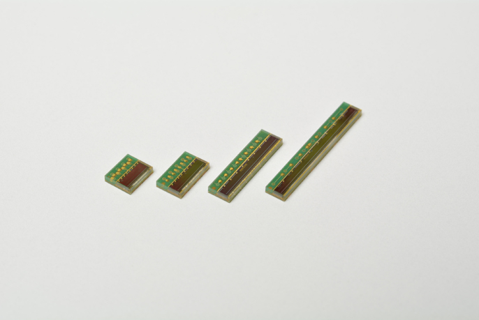
Figure 5. COB packaged CMOS linear image sensors
Another feature of CMOS image sensors where significant improvements can be observed is packaging. For example, using the COB (chip-on-board) technology, Hamamatsu has been able to build CMOS linear image sensors (Fig. 5) measuring only 0.8 mm in thickness. These sensors are half the thickness of previously available sensors.
These thin COB sensors can be used for barcode readers, encoders and various types of image scanning applications including handheld scanners and other devices that need to integrate compact and cost-effective image sensors.
CMOS area image sensors
Advances in CMOS technology have also brought to the market CMOS area image sensors that can be used for industrial and security applications. For example, CMOS area image sensors series S13100 (Fig. 6) newly released by Hamamatsu are offered in SXGA format (1280 x 1024 pixels), VGA format (640 x 480 pixels), and QVGA format (320 x 240 pixels).
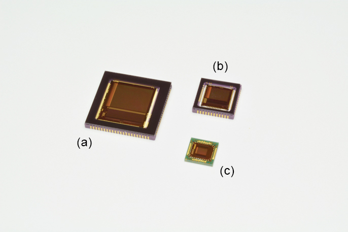
Figure 6. CMOS area image sensors with SXGA (a), VGA (b) and QVGA (c) pixel format
These active pixel sensors include a 2D photodiode array, a vertical decoder, a horizontal decoder, a correlated double sampling (CDS) circuit, a timing generator, an amplifier, a bias circuit, one or several A/D converters, a parallel output signal interface, and a serial peripheral interface (SPI).
Hamamatsu CMOS area image sensors can perform a rolling or global shutter function and high-speed readout function of a selected region of interest (ROI).
The SXGA sensor includes column dedicated A/D converters and a 15-channel LVDS output interface. This sensor can achieve a maximum frame rate of 146 fps (frames per second).
Both the VGA and QVGA sensors include an integrated A/D converter and a 12-bit parallel output interface. The maximum frame rate of the VGA and QVGA sensors are 78 fps and 386 fps, respectively. The QVGA sensor also includes an improved sample-and-hold circuit that allows increasing readout frame rate when a smaller ROI is selected. For example, when a 64 x 64 pixels ROI is selected, a 6890 fps frame rate can be achieved.
These sensors can be used for various industrial applications including machine vision, coin detection, fingerprint pattern imaging, as well as for vein pattern imaging and other medical imaging applications. Since these sensors are sensitive in the near-infrared (NIR) region, they also can be used for different NIR security applications, as well as for position and shape recognition applications.
Custom-designed CMOS image sensors
In addition to its standard CMOS linear and area image sensors, Hamamatsu also offers custom-designed CMOS image sensors that perform special functions required by the customer’s applications.
Conclusion
Over the last decade, CMOS image sensor technology has experienced great progress. Not only have CMOS image sensors been able to penetrate and gain ground in markets previously dominated by CCD sensors, but they have also found new and original applications.
References
- G.C. Holst and T.S. Lomheim, CMOS/CCD Sensors and Camera Sensors, JCD Publishing and SPIE Press (2007).
- M. Muramatsu et al., Greater than 90% QE in Visible Spectrum Perceptible from UV to near IR Hamamatsu Thinned Back Illuminated CCD’s, Proc. SPIE 3019, 2 (April 1997).
- A. Theuwissen, CMOS Image Sensors: State-of-the-art, Solid-State Electronics, Vol 52 (2008).
- T. Rasmussen, Comparison of Sony ILX511B CCD and Hamamatsu S11639 CMOS for UV-VIS spectroscopy, Ibsen Photonics A/S (2014).
- W. Neumann, Fundamentals of Dispersive Optical Spectroscopy Systems, SPIE Press (2014).
Notes
A version of this article was published in the September 2015 issue of Photonics Spectra.
- Confirmation
-
It looks like you're in the . If this is not your location, please select the correct region or country below.
You're headed to Hamamatsu Photonics website for US (English). If you want to view an other country's site, the optimized information will be provided by selecting options below.
In order to use this website comfortably, we use cookies. For cookie details please see our cookie policy.
- Cookie Policy
-
This website or its third-party tools use cookies, which are necessary to its functioning and required to achieve the purposes illustrated in this cookie policy. By closing the cookie warning banner, scrolling the page, clicking a link or continuing to browse otherwise, you agree to the use of cookies.
Hamamatsu uses cookies in order to enhance your experience on our website and ensure that our website functions.
You can visit this page at any time to learn more about cookies, get the most up to date information on how we use cookies and manage your cookie settings. We will not use cookies for any purpose other than the ones stated, but please note that we reserve the right to update our cookies.
1. What are cookies?
For modern websites to work according to visitor’s expectations, they need to collect certain basic information about visitors. To do this, a site will create small text files which are placed on visitor’s devices (computer or mobile) - these files are known as cookies when you access a website. Cookies are used in order to make websites function and work efficiently. Cookies are uniquely assigned to each visitor and can only be read by a web server in the domain that issued the cookie to the visitor. Cookies cannot be used to run programs or deliver viruses to a visitor’s device.
Cookies do various jobs which make the visitor’s experience of the internet much smoother and more interactive. For instance, cookies are used to remember the visitor’s preferences on sites they visit often, to remember language preference and to help navigate between pages more efficiently. Much, though not all, of the data collected is anonymous, though some of it is designed to detect browsing patterns and approximate geographical location to improve the visitor experience.
Certain type of cookies may require the data subject’s consent before storing them on the computer.
2. What are the different types of cookies?
This website uses two types of cookies:
- First party cookies. For our website, the first party cookies are controlled and maintained by Hamamatsu. No other parties have access to these cookies.
- Third party cookies. These cookies are implemented by organizations outside Hamamatsu. We do not have access to the data in these cookies, but we use these cookies to improve the overall website experience.
3. How do we use cookies?
This website uses cookies for following purposes:
- Certain cookies are necessary for our website to function. These are strictly necessary cookies and are required to enable website access, support navigation or provide relevant content. These cookies direct you to the correct region or country, and support security and ecommerce. Strictly necessary cookies also enforce your privacy preferences. Without these strictly necessary cookies, much of our website will not function.
- Analytics cookies are used to track website usage. This data enables us to improve our website usability, performance and website administration. In our analytics cookies, we do not store any personal identifying information.
- Functionality cookies. These are used to recognize you when you return to our website. This enables us to personalize our content for you, greet you by name and remember your preferences (for example, your choice of language or region).
- These cookies record your visit to our website, the pages you have visited and the links you have followed. We will use this information to make our website and the advertising displayed on it more relevant to your interests. We may also share this information with third parties for this purpose.
Cookies help us help you. Through the use of cookies, we learn what is important to our visitors and we develop and enhance website content and functionality to support your experience. Much of our website can be accessed if cookies are disabled, however certain website functions may not work. And, we believe your current and future visits will be enhanced if cookies are enabled.
4. Which cookies do we use?
There are two ways to manage cookie preferences.
- You can set your cookie preferences on your device or in your browser.
- You can set your cookie preferences at the website level.
If you don’t want to receive cookies, you can modify your browser so that it notifies you when cookies are sent to it or you can refuse cookies altogether. You can also delete cookies that have already been set.
If you wish to restrict or block web browser cookies which are set on your device then you can do this through your browser settings; the Help function within your browser should tell you how. Alternatively, you may wish to visit www.aboutcookies.org, which contains comprehensive information on how to do this on a wide variety of desktop browsers.
5. What are Internet tags and how do we use them with cookies?
Occasionally, we may use internet tags (also known as action tags, single-pixel GIFs, clear GIFs, invisible GIFs and 1-by-1 GIFs) at this site and may deploy these tags/cookies through a third-party advertising partner or a web analytical service partner which may be located and store the respective information (including your IP-address) in a foreign country. These tags/cookies are placed on both online advertisements that bring users to this site and on different pages of this site. We use this technology to measure the visitors' responses to our sites and the effectiveness of our advertising campaigns (including how many times a page is opened and which information is consulted) as well as to evaluate your use of this website. The third-party partner or the web analytical service partner may be able to collect data about visitors to our and other sites because of these internet tags/cookies, may compose reports regarding the website’s activity for us and may provide further services which are related to the use of the website and the internet. They may provide such information to other parties if there is a legal requirement that they do so, or if they hire the other parties to process information on their behalf.
If you would like more information about web tags and cookies associated with on-line advertising or to opt-out of third-party collection of this information, please visit the Network Advertising Initiative website http://www.networkadvertising.org.
6. Analytics and Advertisement Cookies
We use third-party cookies (such as Google Analytics) to track visitors on our website, to get reports about how visitors use the website and to inform, optimize and serve ads based on someone's past visits to our website.
You may opt-out of Google Analytics cookies by the websites provided by Google:
https://tools.google.com/dlpage/gaoptout?hl=en
As provided in this Privacy Policy (Article 5), you can learn more about opt-out cookies by the website provided by Network Advertising Initiative:
http://www.networkadvertising.org
We inform you that in such case you will not be able to wholly use all functions of our website.
Close